Technology: gpdk-related process setting
Default process
The technology in gpdk holds a number of common configuration files dealing with process and layout display, such as:
Process layers definitions:
layers.pyLayers display settings:
display.pyLayout pattern accuracy setting:
metrics.pyWaveguide type definitions:
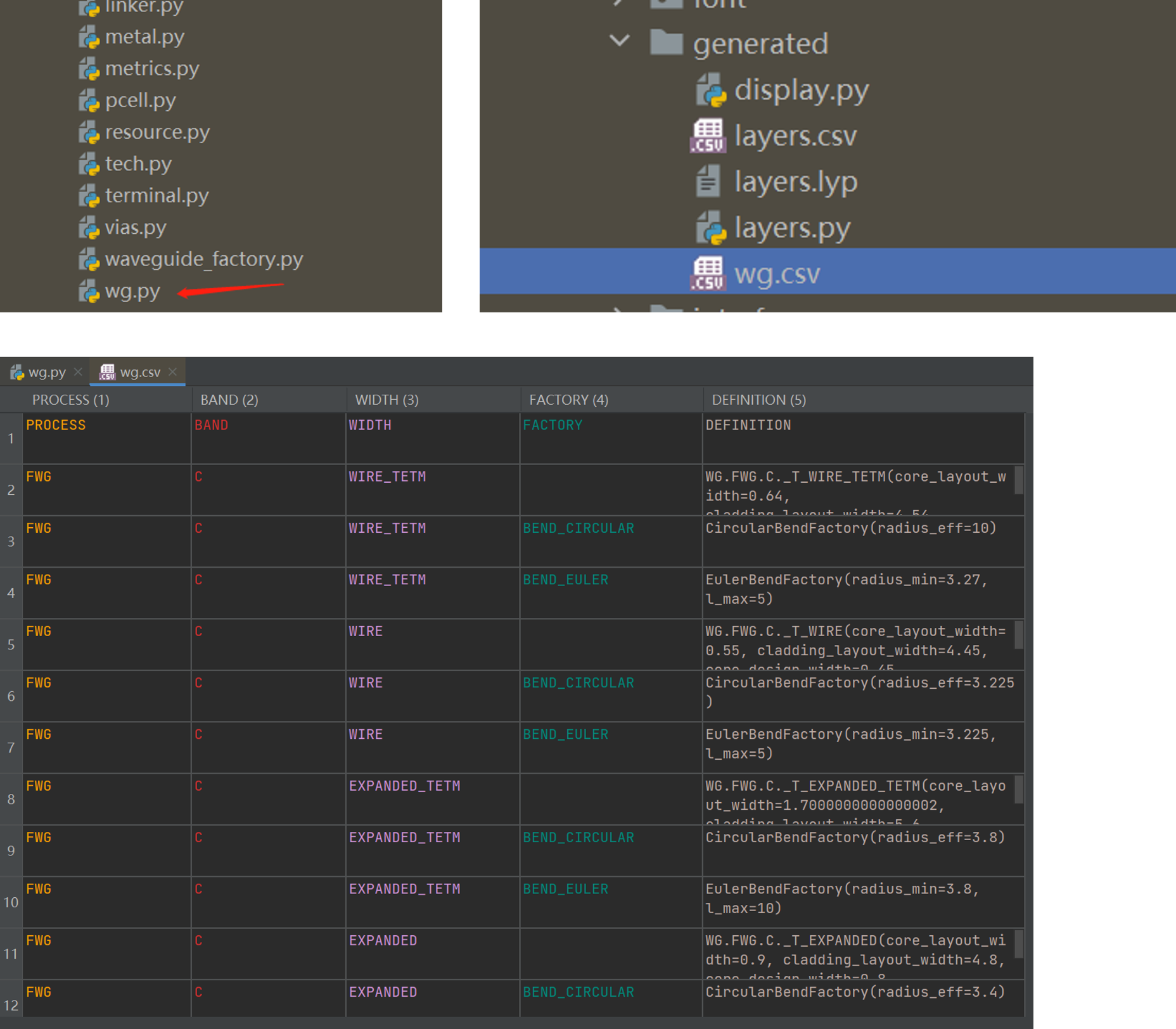
wg.pyRouting-related settings definition:
auto_link.pyAutomatic waveguide type transition:
auto_transition.pyWaveguide corner customization:
auto_bend.pyMetal wiring related settings:
auto_via.py,fitting_function.py
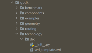
Note: The drc subfolder of technology contains the design rule check template based on the current process generated layout, the CalibreTM DRC rule deck template script.
Customized process
In order to be more convenient for users to use and customize the process information, mainly for layers.py and display.py, technology provides a convenient user-defined file layers.csv file, users can open gpdk > technology > layers.csv file to customize their relevant processes.
First double-click on the file to open the table as shown below:
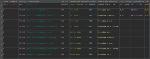
LAYERandDATATYPEtogether determine the number of the layer.NAMEis used to define the name of the layer.DESCRIPTIONis the description of the layer.PROCESSandPROCESS_DESCRIPTIONare used to define and describe the etching process, respectively.PURPOSEandPURPOSE_DESCRIPTIONare used to define and describe the processing process respectively.FILL_COLORis used to define the color of the filled layer.FILL_PATTERNis used to define the graphics of the filled layer, mainlydiagonalandback-diagonal.STROKE_COLORis used to define the color of the border of the layer.
All these information are user-defined.
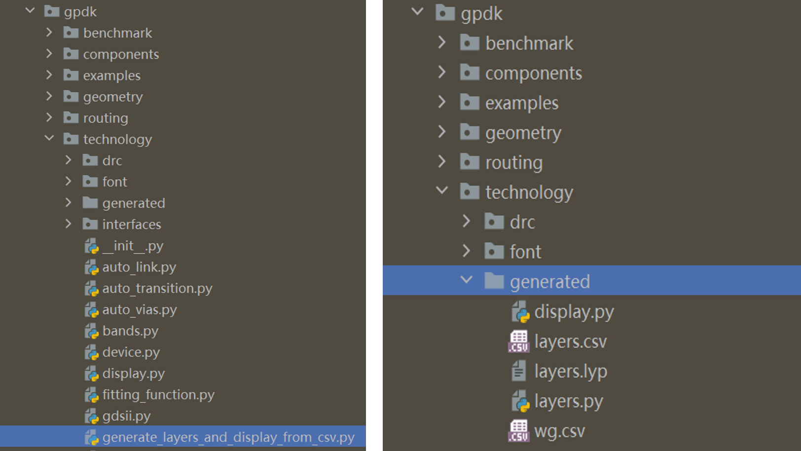
Then after the user has customized the relevant process information, running gpdk > technology > generate_layers_display_from_csv.py directly will generate the generated folder in gpdk > technology, which contains the display.py, layers.csv, layers.lyp, layers.py, and wg.csv files.
Finally, we can use the relevant process setup files generated in the file via gpdk > technology > tech.py . Double-click to open the tech.py file to reveal the following scripts:
from .auto_link import LINKING_POLICY
from .auto_transition import AUTO_TRANSITION
from .auto_vias import AUTO_VIAS
from .bands import BAND
from .device import DEVICE
from .display import DISPLAY
from .fitting_function import FITTING_FUNCTION
from .gdsii import GDSII
from .label import LABEL
from .layers import LAYER, PROCESS, PURPOSE
from .linker import LINKER
from .metal import METAL
from .metrics import METRICS
from .terminal import PIN, PORT
from .vias import VIAS
from .wg import WG
from .resource import RESOURCE
In the module import section we replace the original:
from .display import DISPLAY
from .layers import LAYER, PROCESS, PURPOSE
to:
from .gennerated.display import DISPLAY
from .gennerated.layers import LAYER, PROCESS, PURPOSE
Save it again and then you can use the custom process information.
Waveguide information
In order to be more convenient for users to view the information of the waveguide process in use, technology provides a convenient method to reverse the python source file to generate a csv netlist file, users can open gpdk > technology > wg.py and run it, then the wg.csv file will be generated in the generate folder, you can open the file to quickly view various information related to waveguide.