Create a CUSTOM PDK
This chapter is designed to help users quickly create PDKs that use their own process flows to automate layout routing. A customized PDK must have the following files to configure their settings to PhotoCAD.
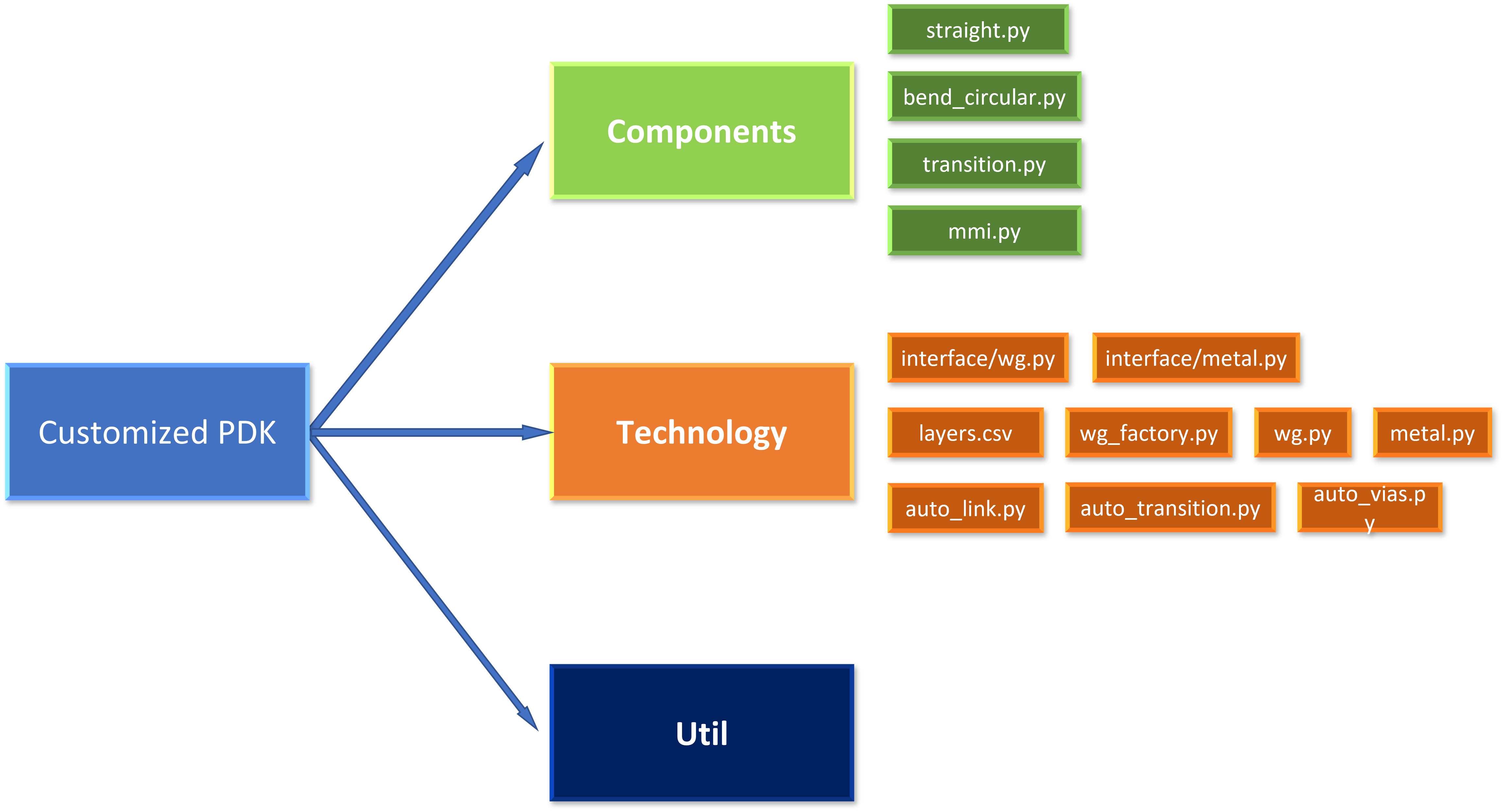
Contents:
components:Store base passive and active components e.g., straight waveguides, circular bends, waveguide transitions, MMIs, heaters.
technology:PDK technology setting such as waveguide settings, automatic waveguide routing settings, layer information.
util:some useful function.
Standard Procedure
Configure CAD layer information (layer ID/datatype/layer name) in layers.csv.
Add waveguide information(waveguide type/wg width/wg layer) in wg.py but keep straight factory and bend factories blank.
Create basic components such as straight waveguide, bends, taper, transitions in component folder.
Assign straight factory and bend factory in every waveguide in wg.py.
Configure taper and transition components in auto_transition.py.
Set up
LINKING_POLICYin :ref:auto_link.pyto easily connect waveguides with bends and connections.Build
linker.pysettings to assign designated waveguide with designated length, bends and transitions.After
LINKERorLinkBetweenworks in your PDK, try to create more components and build up a real photonic integrated circuit by using various function in PhotoCAD.