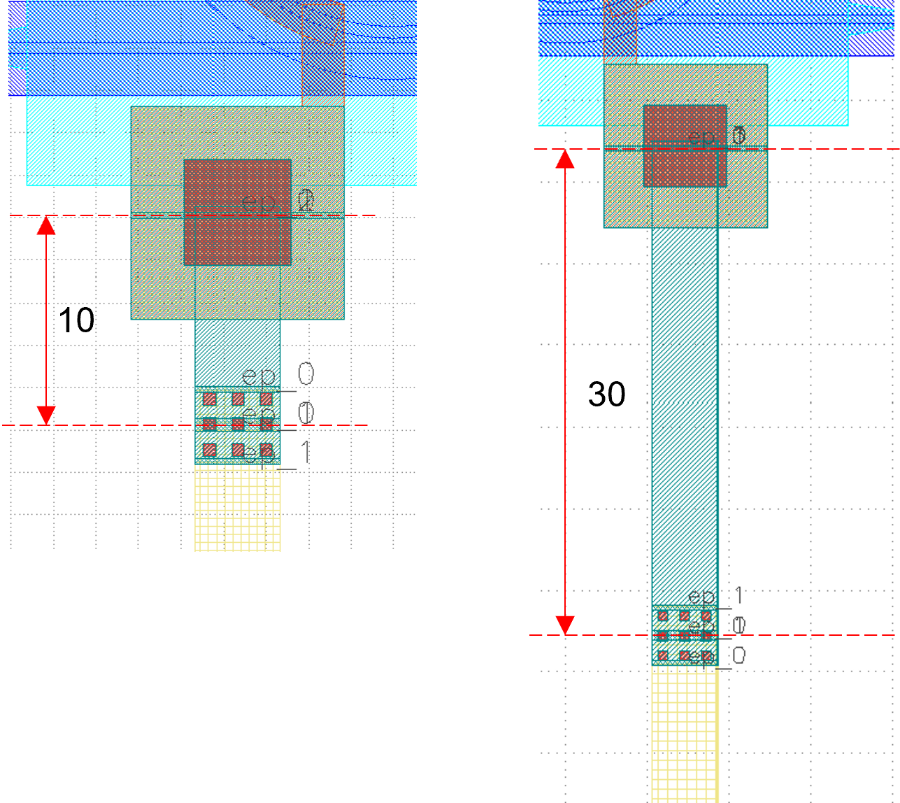
PhotoCAD
  • Introduction
    • PhotoCAD Introduction
      • fnpcell
      • link
  • Installation
    • Installing PhotoCAD
      • System Requirement
      • Install Python IDE and Python package
      • Install PhotoCAD
      • PhotoCAD file structure
  • PhotoCAD Hands-on
  • gpdk (generic PDK)
    • Components: gpdk built-in components
      • Passive components
      • Active components
    • Examples: gpdk built-in examples
    • Routing: gpdk built-in routing method
    • Technology: gpdk-related process setting
      • Default process
      • Customized process
      • Waveguide information
    • layout01: Project Development
  • fnpcell
    • Definition of each component class in fnpcell
      • Full script
      • Section Script Description
    • The use of classes in fnpcell (generating components)
      • Section Script Description
    • Example of using fnpcell to build class
      • Example1: bend_bezier.py
        • Full script
        • Section Script Definition
      • Example2: bend_circular.py
        • Full script
        • Section Script Definition
    • Design Rule Check(DRC)
      • Generate SVRFTM template
      • Generate DRC template files using SVRFTM templates
        • Full script
        • Section Script Definition
      • Using DRC template files
      • Format instructions
    • Writing a user-defined PCell in PhotoCAD
      • Import module
      • Define RingResonator
      • Define RingResonator2
      • Create examples(layout units) using classes RingResonator and RingResonator2
      • GDS Layout

Guides

  • Create a Parametrized Cell(PCell)
    • Create shapes and boundaries
      • fp.el API
        • fp.el
      • fp.g API
        • fp.g
    • Default values for PCell Parameters
      • Ways to implement default values for PCell parameter
    • Define Ports/Pins
      • Ports/Pins from existing PCells
      • Manually adding Ports/Pins
        • Full Script
        • Section Script Description
        • View the layout
    • Generate array of cells
      • new_array
        • Full script
        • Section Script Description
        • Export GDS Layout
    • List of gpdk components
      • BendEuler
        • Full script
        • Section Script Description
        • Extend PCells from BendEuler
        • Export GDS Layout
      • Taper
        • Full script
        • Section Script Description
        • Extension of the taper ports
      • Splitter
        • Full Script
        • Section Script Description
        • Run the script and view the layout
      • Directional Coupler Bend
        • Full script
        • Parameter description
      • Ring filter
        • Full script
        • Parameters and testing descriptions
      • Elliptical Rings
        • Full script
        • fp.el.Ring Description
        • fp.el.EllipticalRing Description
      • Phase Shifter
        • Full script
        • Segment Description
          • 1. Import function module
          • 2. Main function
          • 3. Define function
      • Sampler Periodic
        • Full script
        • Left graph
        • Right graph
      • Mach-Zehnder modulator
        • Full Script
        • Section Script Description
        • Export GDS Layout
      • Grating Coupler with linecap
        • Full script
          • Section Script Description
          • Run the script and view the layout
  • Create a CUSTOM PDK
    • technology
      • layers.csv
      • waveguide factory.py
        • Straight
        • CircularBend
        • Implementation
      • wg.py
        • waveguide configuration
        • Define parameters in each waveguide types
        • Generate waveguide class
        • Generate wg information to csv file
      • auto_transition.py
        • Create transition components
        • Set up transition settings
        • Example
      • auto_link.py
        • LESS_TRANS
        • MAX_SWG
        • Usage
      • linker.py
    • components
      • Straight
      • bend_circular
      • Taper
      • Transition
      • grating_coupler
      • MMI
    • Standard Procedure
      • technology
        • layers.csv
        • waveguide factory.py
          • Straight
          • CircularBend
          • Implementation
        • wg.py
          • waveguide configuration
          • Define parameters in each waveguide types
          • Generate waveguide class
          • Generate wg information to csv file
        • auto_transition.py
          • Create transition components
          • Set up transition settings
          • Example
        • auto_link.py
          • LESS_TRANS
          • MAX_SWG
          • Usage
        • linker.py
      • components
        • Straight
        • bend_circular
        • Taper
        • Transition
        • grating_coupler
        • MMI
  • Design a circuit
    • Common used transformation
      • place
      • translated
      • scaled
      • rotated
      • mirrored
    • Waveguide Routing
      • Single-port to Single-port
        • Examples
      • Multi-port to Multi-port
        • fp.Linked example ( Recommendation★★★ )
        • fp.create_links example ( Recommendation★★★★★ )
      • Routing Path Selection
        • waylines
          • Absolute control points provided
          • Relative control points provided
        • waypoints
        • target_length
    • Electrical wire Routing
      • Link Electrical Pad
        • Full script
        • Parameters and testing descriptions
        • Connections
          • Top connection
          • Middle connection
          • Bottom connection
      • Link Electrical pad with turning angle
        • Full script
        • Parameters and testing description
          • Components positioning
    • Advanced Waveguide Routing
      • Routing in batch form
        • Components Scan
          • Full script
          • Section Script Definition
        • Importing python libraries and functional modules of PhotoCAD
        • Define device adaptation, fiber coupling, constant fiber coupler and several other classes
        • Define the batch class Block
        • Define Alignment
        • Define Title
        • Define Blank
        • Define method to get the port center
        • Define methods for obtaining module content
        • Define CompScan
        • Define CompScanBuilder
        • Create the component and export the layout
          • Script Description
          • GDS Layout
      • Extension of the ports
      • Extended
        • Full script
        • Section Script Definition
          • Create extended ports and export layout
        • GDS Layout
      • Expand the footprint for downstream devices
      • HFanout
        • Full script
        • Section Script Definition
          • Importing libraries and modules
          • Define HFanout
          • Create components and export layouts
        • GDS Layout
      • Horizontalization of device ports
      • Horizontalized
        • Full script
        • Section Script Definition
          • Create horizontalized components ports and export layouts
        • GDS Layout
      • LinkBetween
        • Import function module
        • Main function
        • Define function
        • Test for waypoints in LinkBetween
      • Routing automation between components ports
        • Linked
          • Full Script
          • Section Script Description
        • AutoTransitioned
      • LinkSmooth
        • Full script
    • Design rule check(DRC)
      • What is DRC?
        • Exclusion
        • Inclusion
        • Minimum_width
      • DRC check in KLayout
        • View designs in KLayout
        • Import DRC file to KLayout
        • View design rule errors
        • Make adjustments or waive the error
      • Examples files to test your knowledge
  • Post Layout Simulation
    • Component level simulation model
      • WGModel class
      • Script description
      • Other simulation models
    • MZI post-simulation
      • Full script
      • Build simulation models for WG, DC
      • Implement simulation models to components
      • Build MZI circuit and define poet-simulation functions
      • Generate GDS file and run post-simulation
  • Useful function when scripting PhotoCAD
    • Placing PCell ports
    • Get PCell information
      • Get PCell name
      • Get PCell region
      • Get ports information
      • Get two points relative information
    • Boolean operations between elements and layers
      • Boolean with different layers
      • Boolean with elements
    • Importing/Exporting GDS/Json file
      • Import GDS file
      • Export GDS file
      • Export Json file
    • Simplify layout by fp.use_sketch_view
      • Implement fp.use_sketch_view
      • Different usage of fp.use_sketch_view
      • GDS file build-time results
      • Example Scripts
    • Manually add ports/pins on PCells
    • Get the coordinates of the cell
    • Change the cell name in GDS file
      • Cell naming rules
    • Pytest: Prevent unexpected changes to the layout
      • Accidental modification of PCell with completed design
      • Accidental modification of other shared methods
    • Max-Optics simulation interface: runner.py
      • Interface usage:
      • Interface script description:
  • Quick Start: Create a Circuit
    • Step 1: Build basic building blocks
      • Bend
      • Straight
      • Taper
    • Step 2: Build basic circuits with basic building blocks
      • DirectionalCoupler
      • MMI
    • Step 3: Build complex circuits using basic building blocks
      • target_length
      • waypoints
      • waylines
    • Step 4: Drawing of common shapes and layout design by Boolean operations
      • Commonly_used_shape
        • Rectangle
        • Circle
        • Polygon
        • Ring
        • Regular_Polygon
      • Boolean_operation
        • OR
        • AND
        • NOT
        • XOR
        • Examples
    • Step 5: Example(MMI Tree)

Examples

  • Programmable Photonic Integrated Circuit
    • Part I. Building a Rectangular Network
    • Part II. Parameter Description
    • Part III. Test Description
    • Part IV. Summary
  • Triangle MZI mesh
    • Part I. Build MZI units
    • Part II. Build programmable triangular MZI mesh
      • MZI Mesh with 8 external optical ports (MZI_triangle_mesh)
      • MZI Mesh with 8 Grating Couplers (MZI_triangle_mesh_with_GC)
      • Triangle MZI array (MZI_triangle_array)
  • Demultiplexer
    • Full script
    • View GDS layout file
    • Instantiation of components
    • Testing and Analysis
    • Get Pcells information via get
    • Summary
  • Cascaded Mach-Zehnder (CMZ) wavelength filter
    • Implement simulation models for auto-link
    • Wavelength Splitters
    • CMZ wavelength demultiplexer
  • Visualize in Jupyter Notebook
    • MZI circuit layout generation in Jupyter notebook
      • Create a Jupyter Notebook
      • Code cell & Markdown cell
      • Generate MZI layout

Support and Changelog

  • fnpcell API
    • Commonly used interface
      • Graphics
      • Routing
      • Transform
      • Information
    • PCell Parameters
      • Classes
      • AnchorParam
      • BooleanParam
      • DegreeParam
      • DeviceParam
      • FloatParam
      • IParam
      • IntParam
      • LayerParam
      • ListParam
      • MappingParam
      • MetalLineTypeParam
      • NameListParam
      • NameParam
      • NonNegFloatParam
      • NonNegIntParam
      • Param
      • PointsParam
      • PortOptionsParam
      • PositionParam
      • PositiveFloatParam
      • PositiveIntParam
      • SetParam
      • TextParam
      • TransformParam
      • WaveguideTypeParam
  • Release notes
    • PhotoCAD V1.5.0
    • PhotoCAD V1.6.0
  • Frequently Asked Questions
    • Data Compression
    • Smooth curve for routing using bend_factory
    • Differences between __post_pcell_init__ & __post_init__
  • About Us
PhotoCAD
  • Design a circuit
  • Electrical wire Routing
  • Link Electrical Pad
  • View page source

Link Electrical Pad

Full script

from fnpcell import all as fp
from gpdk import all as pdk
from gpdk.technology import get_technology

@fp.pcell_class()

class LinkedElec(fp.PCell):
    def build(self):
        insts, elems, ports = super().build()
        TECH = get_technology()

        rm1 = pdk.RingFilter(waveguide_type=TECH.WG.FWG.C.WIRE)
        rm2 = pdk.RingFilter(waveguide_type=TECH.WG.FWG.C.WIRE)

        rm1 = rm1.translated(-200, 100)
        rm2 = rm2.translated(200, 100)

        MT_2 = TECH.METAL.MT.W10.updated(line_width=2)
        MT_4 = TECH.METAL.MT.W10.updated(line_width=4)
        M2_4 = TECH.METAL.M2.W10.updated(line_width=4)
        to = fp.Waypoint
        device = fp.Linked(
            metal_line_type=MT_2,
            metal_min_distance=20,
            links=[
                rm1["op_3"] >> to(0, 150, -90) >> rm2["op_0"],
                rm1["ep_1"].with_orientation(degrees=-90) >> to(0, -10, -90) >> rm2["ep_0"].with_orientation(degrees=-90),
                fp.LinkBetween(
                    rm1["ep_0"].with_orientation(degrees=-90),
                    rm2["ep_1"].with_orientation(degrees=-90),
                    start_distance=40,
                    # waypoints=[to(-50, -100, -90)],
                    # waypoints=[fp.Offset.until_y(-50), fp.Offset.until_x(-20), fp.Offset.until_y(-30)],
                    waypoints=[fp.Offset.until_y(50), fp.Offset.until_x(-20), fp.Offset.until_y(-30)],
                    metal_line_type=[(0, MT_4), (10, M2_4), (-30, MT_4)],
                ),
            ],
            ports=[],  # [sb10["op_0"], s40["op_1"]],
        )
        insts += device
        return insts, elems, ports
if __name__ == "__main__":
    from pathlib import Path
    gds_file = Path(__file__).parent / "local" / Path(__file__).with_suffix(".gds").name
    library = fp.Library()
    TECH = get_technology()
    # =============================================================
    # fmt: off
    library += LinkedElec()
    # fmt: on
    # =============================================================
    fp.export_gds(library, file=gds_file)
    fp.plot(library)

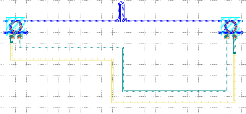
Run the complete script once and generate the following GDS layout.

../_images/10.1.png

Parameters and testing descriptions

Call pdk.RingFilter to generate a RingFilter with two default structure parameters, specifying the waveguide type as TECH.WG.FWG.C.WIRE; then use .translated command to place the two devices at (-200,100) and (200,100).

rm1 = pdk.RingFilter(waveguide_type=TECH.WG.FWG.C.WIRE)
rm2 = pdk.RingFilter(waveguide_type=TECH.WG.FWG.C.WIRE)

rm1 = rm1.translated(-200, 100)
rm2 = rm2.translated(200, 100)

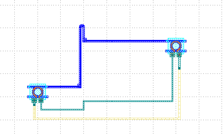
We change rm1 = rm1.translated(-200, 100) to rm1 = rm1.translated(-100, 0) and run it to get the following layout. As you can see from the figure below, despite the change in the position of the left device, PhotoCAD is still able to connect the wiring automatically due to its powerful auto-routing feature.

../_images/10.2.png

Connections

The lower code section is responsible for how the devices are connected to each other.

to = fp.Waypoint
        device = fp.Linked(
            metal_line_type=MT_2,
            metal_min_distance=20,
            links=[
                rm1["op_3"] >> to(0, 150, -90) >> rm2["op_0"],
                rm1["ep_1"].with_orientation(degrees=-90) >> to(0, -10, -90) >> rm2["ep_0"].with_orientation(degrees=-90),
                fp.LinkBetween(
                    rm1["ep_0"].with_orientation(degrees=-90),
                    rm2["ep_1"].with_orientation(degrees=-90),
                    start_distance=40,
                    # waypoints=[to(-50, -100, -90)],
                    # waypoints=[fp.Offset.until_y(-50), fp.Offset.until_x(-20), fp.Offset.until_y(-30)],
                    waypoints=[fp.Offset.until_y(50), fp.Offset.until_x(-20), fp.Offset.until_y(-30)],
                    metal_line_type=[(0, MT_4), (10, M2_4), (-30, MT_4)],
                ),
            ],
            ports=[],  # [sb10["op_0"], s40["op_1"]],
        )

Top connection

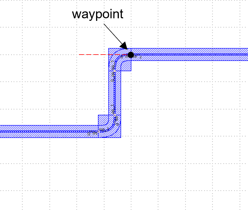
rm1["op_3"] >> to(0, 150, -90) >> rm2["op_0"]``means that the ``op_3 port of rm1 is connected to the op_0 port of rm2, and the connection path needs to pass through the point (0,150), where -90 means the direction of the waveguide port at the path point, we change -90 to 0 and run the program once to get the following figure :

../_images/10.3.png

We then compare with the original -90° and 90° angle:

90°: .. image:: ../example_image/10.4.png

-90°: .. image:: ../example_image/10.4-2.png

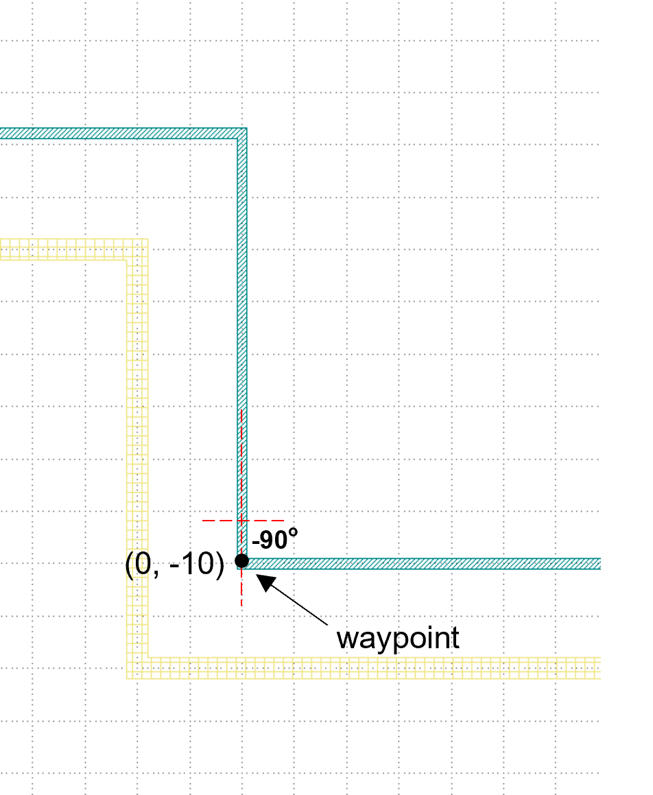
From the above comparison, it can be analyzed that the specified angle is the angle between the line passing in front of the waypoint and the horizontal direction, and the degree is exactly from bottom to top, which means the degree is negative from top to bottom.

Middle connection

We modify the degrees in rm1["ep_1"].with_orientation(degrees=-90) to 0 degrees to get the figure on the right below, which shows that degrees is the direction when changing the connection of op_1 (0° with 360° facing right, 90° with -270° facing up, 180° with -180° facing left, and 270° with -90° facing down; similar to the usual angles in the four quadrants of the X-Y coordinate system).

../_images/10.5.png

Let’s continue to test the angle of the path point, starting with the initial -90° and running it to get the following figure, which shows that the line is coming down from above the waypoint.

../_images/10.6.png

Bottom connection

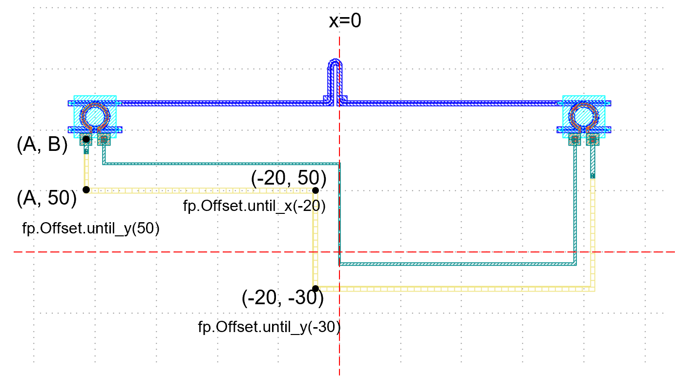
The code below controls the direction of the routing. until_x and until_y are commonly understood to mean that the direction of the line is not changed (i.e., horizontal or vertical coordinates), and the horizontal (vertical) coordinates are the turning points of the set values.

waypoints=[fp.Offset.until_y(50), fp.Offset.until_x(-20), fp.Offset.until_y(-30)]

Take the following figure as an example to illustrate. Firstly, the line is extended downward from the point (A, B), and the horizontal coordinates on the line do not change during the extension, while the first command is until_y(50), so the position of the turning point is (A, 50); then, the second command is until_x(-20), and the line is extended to the right, i.e. the vertical coordinates remain unchanged, to reach the turning point (-20, 50); finally, the until_y(-30) command makes the line extend downward to (-20, -30), and then the line is automatically connected to the right end.

../_images/10.7.png

During the connection, we change the type of metal wire with the following command.

metal_line_type=[(0, MT_4), (10, M2_4), (-30, MT_4)]

Starting from the starting point, MT_4 type metal wire specified by 10 μm is used, then M2_4 type metal wire is used between the end of the first section of MT_4 and the position 30 μm below the right-hand port, and the MT_4 type metal wire is used for the wire within 30 μm of the right-hand port.

First of all, the connection is from the left end to the right end, and in that direction is positive, the opposite direction is negative. The parameter 0 in the first bracket in the code refers to the first MT_4 line starting from the position of 0 from the port,``10`` represents the total length of the first MT_4; and -30 refers to the position of 30μm in the reverse direction of the right port (i.e. 30μm below the right end), then the last section of the connecting line is the MT_4 set; the rest of the line is of type M2_4.

../_images/10.8.png
Previous Next

© Copyright 2024, Latitudeds.com.

Built with Sphinx using a theme provided by Read the Docs.