Ring filter
Full script
import math
from typing import Tuple
from fnpcell import all as fp
from gpdk.technology import get_technology
from gpdk.technology.interfaces import CoreCladdingWaveguideType
@fp.pcell_class()
class RingFilter(fp.PCell):
"""
Attributes:
ring_radius: defaults to 10
gap: defaults to 0.2
gap_monitor: defaults to 0.5
waveguide_type: type of waveguide
port_names: defaults to ["op_0", "op_1", "op_2", "op_3", "ep_0", "ep_1"]
Examples:
```python
TECH = get_technology()
ring = RingFilter(name="f1", waveguide_type=TECH.WG.FWG.C.WIRE)
fp.plot(ring)
```

"""
ring_radius: float = fp.PositiveFloatParam(default=10).as_field()
gap: float = fp.PositiveFloatParam(default=0.2).as_field()
gap_monitor: float = fp.PositiveFloatParam(default=0.5).as_field()
waveguide_type: CoreCladdingWaveguideType = fp.WaveguideTypeParam(type=CoreCladdingWaveguideType).as_field()
port_names: fp.IPortOptions = fp.PortOptionsParam(count=6, default=["op_0", "op_1", "op_2", "op_3", "ep_0", "ep_1"]).as_field()
def _default_waveguide_type(self):
return get_technology().WG.FWG.C.WIRE
def build(self) -> Tuple[fp.InstanceSet, fp.ElementSet, fp.PortSet]:
insts, elems, ports = super().build()
TECH = get_technology()
# fmt: off
LAYER = TECH.LAYER
ring_radius = self.ring_radius
gap = self.gap
gap_monitor = self.gap_monitor
waveguide_type = self.waveguide_type
port_names = self.port_names
si_etch2_layer = LAYER.SWG_COR
vl_layer = LAYER.VIA1_DRW
mh_layer = LAYER.TIN_DRW
m1_width = 6.0
m1_enc = 4.25
via_width = 5.0
via_height = 5.0
taper_big_end = 2.0
taper_small_end = 0.3
taper_length = 5.0 # FWG
w_mh = 2.0
min_mh_degrees = -75.0
max_mh_degrees = 255.0
w_m1_out = m1_width
r_m1_out = ring_radius + m1_enc
r_mh = ring_radius
r_mh_in = r_mh - w_mh / 2
w_si_3 = w_m1_out + r_m1_out * 2
h_si_3 = w_si_3
core_width = waveguide_type.core_width
x0 = 0
y0 = ring_radius + gap + core_width
ring = waveguide_type(curve=fp.g.EllipticalArc(radius=ring_radius, origin=(x0, y0))).with_ports((None, None)).with_name("ring")
insts += ring
bus_length = w_si_3 + taper_length * 2
bus = waveguide_type(curve=fp.g.Line(length=bus_length, anchor=fp.Anchor.CENTER, origin=(0, 0))).with_name("bus")
insts += bus
y_offset = ring_radius * 2 + gap + gap_monitor + core_width * 2
monitor = waveguide_type(curve=fp.g.Line(length=bus_length, anchor=fp.Anchor.CENTER, origin=(0, y_offset))).with_name("monitor")
insts += monitor
rect = fp.el.Rect(width=w_si_3, height=h_si_3, layer=si_etch2_layer, origin=(x0, y0))
elems += rect
taper2 = fp.el.Line(length=taper_length, stroke_width=taper_big_end, final_stroke_width=taper_small_end, layer=si_etch2_layer, origin=(x0 + w_si_3 / 2, 0))
elems += taper2
taper3 = fp.el.Line(length=taper_length, stroke_width=taper_big_end, final_stroke_width=taper_small_end, layer=si_etch2_layer, origin=(x0 + w_si_3 / 2, y_offset))
elems += taper3
taper0 = fp.el.Line(length=taper_length, stroke_width=taper_small_end, final_stroke_width=taper_big_end, layer=si_etch2_layer, anchor=fp.Anchor.END, origin=(x0 - w_si_3 / 2, y_offset))
elems += taper0
taper1 = fp.el.Line(length=taper_length, stroke_width=taper_small_end, final_stroke_width=taper_big_end, layer=si_etch2_layer, anchor=fp.Anchor.END, origin=(x0 - w_si_3 / 2, 0))
elems += taper1
ring_mh = fp.el.EllipticalArc(radius=r_mh, stroke_width=w_mh, layer=mh_layer, final_degrees=max_mh_degrees - min_mh_degrees, transform=fp.rotate(degrees=min_mh_degrees).translate(x0, y0))
elems += ring_mh
min_mh_radians = math.radians(min_mh_degrees)
print(min_mh_degrees)
dx = r_mh_in * math.cos(min_mh_radians)
dy = r_mh_in * math.sin(min_mh_radians)
# TODO magic number 10
#VIA1 Layer
v1 = fp.el.Rect(width=via_width, height=via_height, layer=vl_layer, origin=(dx + via_width, -10 + via_height / 2 - core_width / 2))
elems += v1
v2 = fp.el.Rect(width=via_width, height=via_height, layer=vl_layer, origin=(-dx - via_width, -10 + via_height / 2 - core_width / 2))
elems += v2
#M2 Layer
m2 = fp.el.Rect(width=10, height=10, layer=LAYER.M2_DRW, origin=(dx + via_width, -10 + via_height / 2 - core_width / 2))
elems += m2
m2 = fp.el.Rect(width=10, height=10, layer=LAYER.M2_DRW, origin=(-dx - via_width, -10 + via_height / 2 - core_width / 2))
elems += m2
#VIA2 Layer
v1 = fp.el.Rect(width=via_width, height=via_height, layer=LAYER.VIA2_DRW, origin=(dx + via_width, -10 + via_height / 2 - core_width / 2))
elems += v1
v2 = fp.el.Rect(width=via_width, height=via_height, layer=LAYER.VIA2_DRW, origin=(-dx - via_width, -10 + via_height / 2 - core_width / 2))
elems += v2
#MT Layer
mt = fp.el.Rect(width=10, height=10, layer=LAYER.MT_DRW, origin=(dx + via_width, -10 + via_height / 2 - core_width / 2))
elems += mt
mt = fp.el.Rect(width=10, height=10, layer=LAYER.MT_DRW, origin=(-dx - via_width, -10 + via_height / 2 - core_width / 2))
elems += mt
h_mh = y0 + dy + core_width / 2 + via_height / 2
mh1 = fp.el.Rect(width=w_mh, height=h_mh, layer=mh_layer, origin=(dx + w_mh / 2, -core_width / 2 - 2.5 + h_mh / 2))
elems += mh1
mh2 = fp.el.Rect(width=w_mh, height=h_mh, layer=mh_layer, origin=(-dx - w_mh / 2, -core_width / 2 - 2.5 + h_mh / 2))
elems += mh2
# magic number 10
mh1b = fp.el.Rect(width=10, height=10, layer=mh_layer, origin=(-dx - 5, -core_width / 2 - via_height / 2 - 10 / 2))
elems += mh1b
mh2b = fp.el.Rect(width=10, height=10, layer=mh_layer, origin=(dx + 5, -core_width / 2 - via_height / 2 - 10 / 2))
elems += mh2b
top_start_ray, top_end_ray = monitor.curve.end_rays
bottom_start_ray, bottom_end_ray = bus.curve.end_rays
pin1_x, pin1_y = (-dx - via_width, -10 + via_height / 2 - core_width / 2)
pin2_x, pin2_y = (dx + via_width, -10 + via_height / 2 - core_width / 2)
ports += fp.Port(name=port_names[0], position=top_start_ray.position, orientation=top_start_ray.orientation, waveguide_type=waveguide_type)
ports += fp.Port(name=port_names[1], position=bottom_start_ray.position, orientation=bottom_start_ray.orientation, waveguide_type=waveguide_type)
ports += fp.Port(name=port_names[2], position=bottom_end_ray.position, orientation=bottom_end_ray.orientation, waveguide_type=waveguide_type)
ports += fp.Port(name=port_names[3], position=top_end_ray.position, orientation=top_end_ray.orientation, waveguide_type=waveguide_type)
ports += fp.Pin(name=port_names[4], position=(pin1_x, pin1_y), shape=v1.shape, metal_line_type=TECH.METAL.MT.W10)
ports += fp.Pin(name=port_names[5], position=(pin2_x, pin2_y), shape=v2.shape, metal_line_type=TECH.METAL.MT.W10)
# fmt: on
return insts, elems, ports
if __name__ == "__main__":
from pathlib import Path
gds_file = Path(__file__).parent / "local" / Path(__file__).with_suffix(".gds").name
library = fp.Library()
TECH = get_technology()
# =============================================================
# fmt: off
library += RingFilter()
# fmt: on
# =============================================================
fp.export_gds(library, file=gds_file)
fp.plot(library)
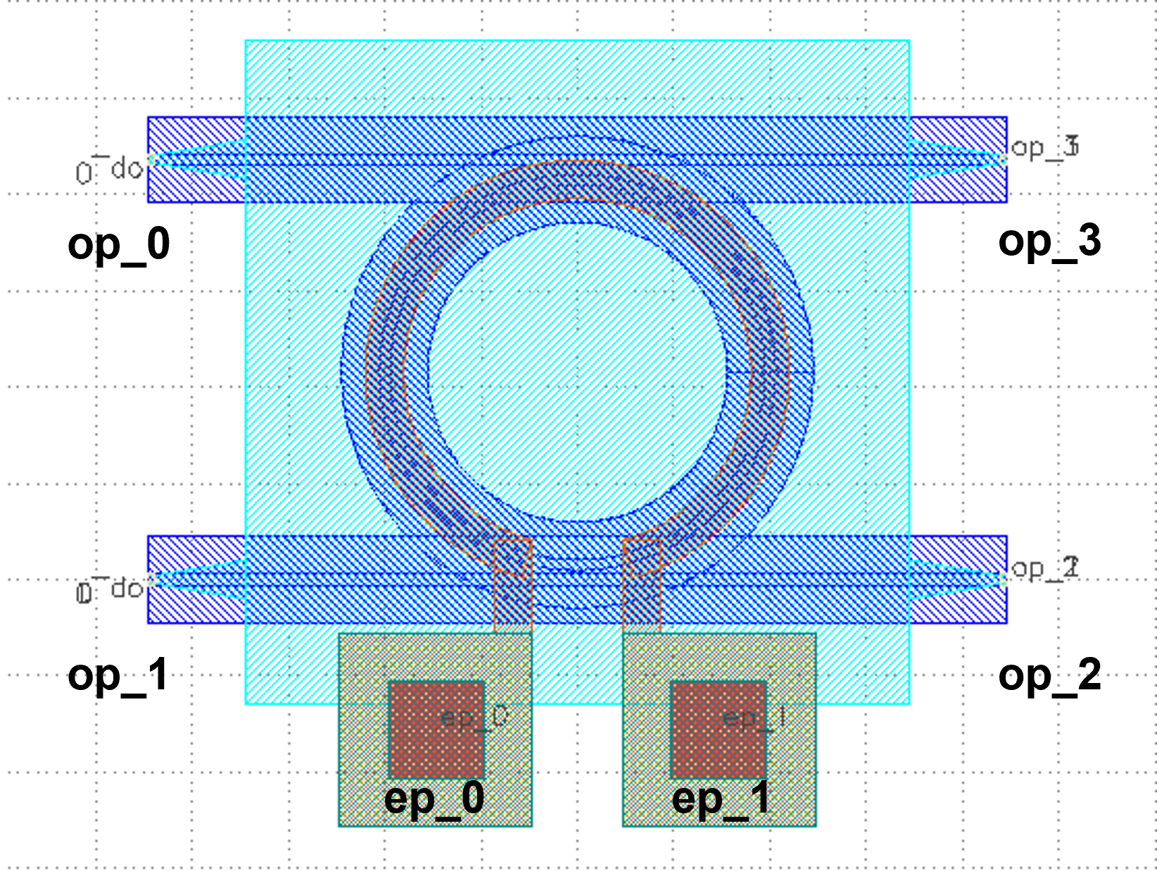
Run the complete script once, generating the following GDS layout.
Parameters and testing descriptions
With the preceding examples as a basis, we will mainly test some key parameters later.
# Define three layers
  si_etch2_layer = LAYER.SWG_COR
vl_layer = LAYER.VIA1_DRW
mh_layer = LAYER.TIN_DRW
# Define several basic parameters of the device
m1_width = 6.0
m1_enc = 4.25
via_width = 5.0
via_height = 5.0
taper_big_end = 2.0
taper_small_end = 0.3
taper_length = 5.0  # FWG
w_mh = 2.0
min_mh_degrees = -75.0
max_mh_degrees = 255.0

w_m1_out = m1_width
r_m1_out = ring_radius + m1_enc
r_mh = ring_radius
r_mh_in = r_mh - w_mh / 2

w_si_3 = w_m1_out + r_m1_out * 2
h_si_3 = w_si_3
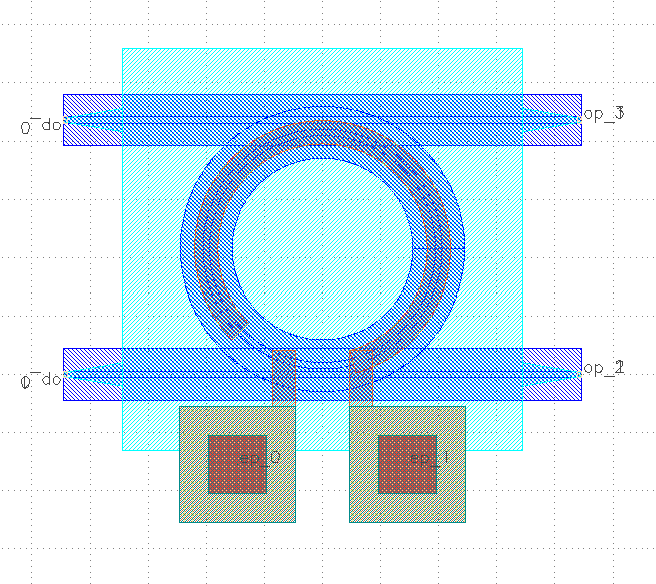
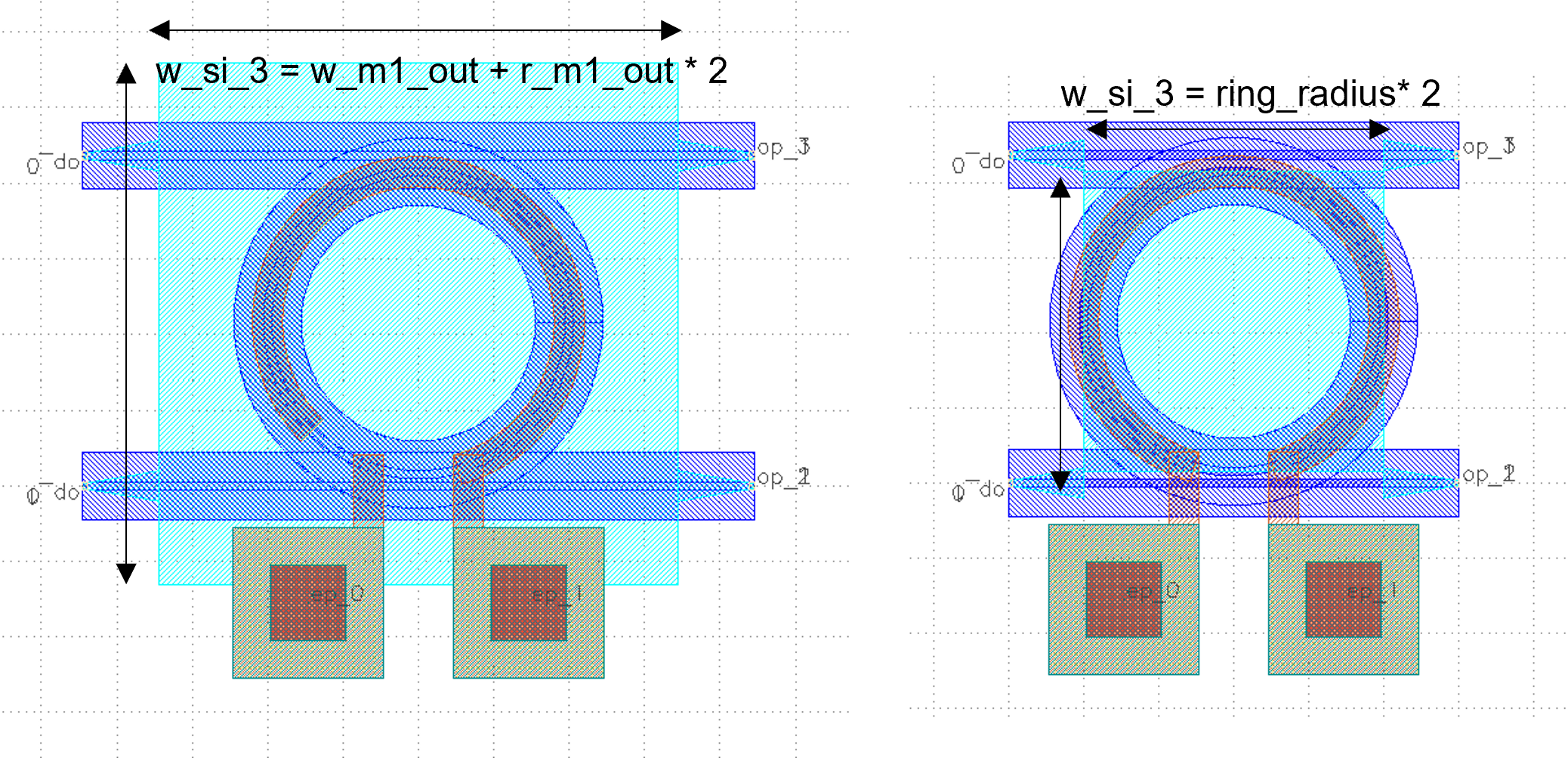
In the above code, w_si_3 is equal to h_si_3, below we change w_si_3 to :
w_si_3 = ring_radius * 2
h_si_3 = w_si_3
Run to obtain the following layout.
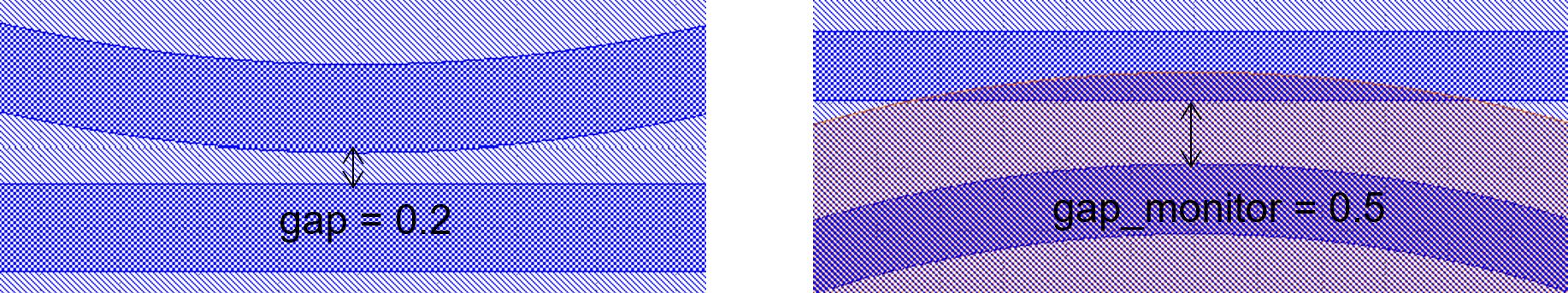
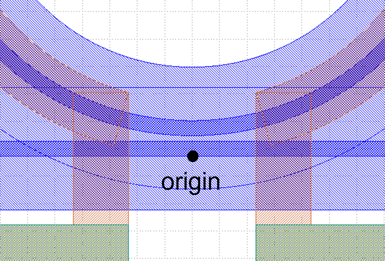
gap and gap_monitor control the gaps labeled in the figure below, respectively, with gap controlling the bottom and gap_monitor controlling the top.
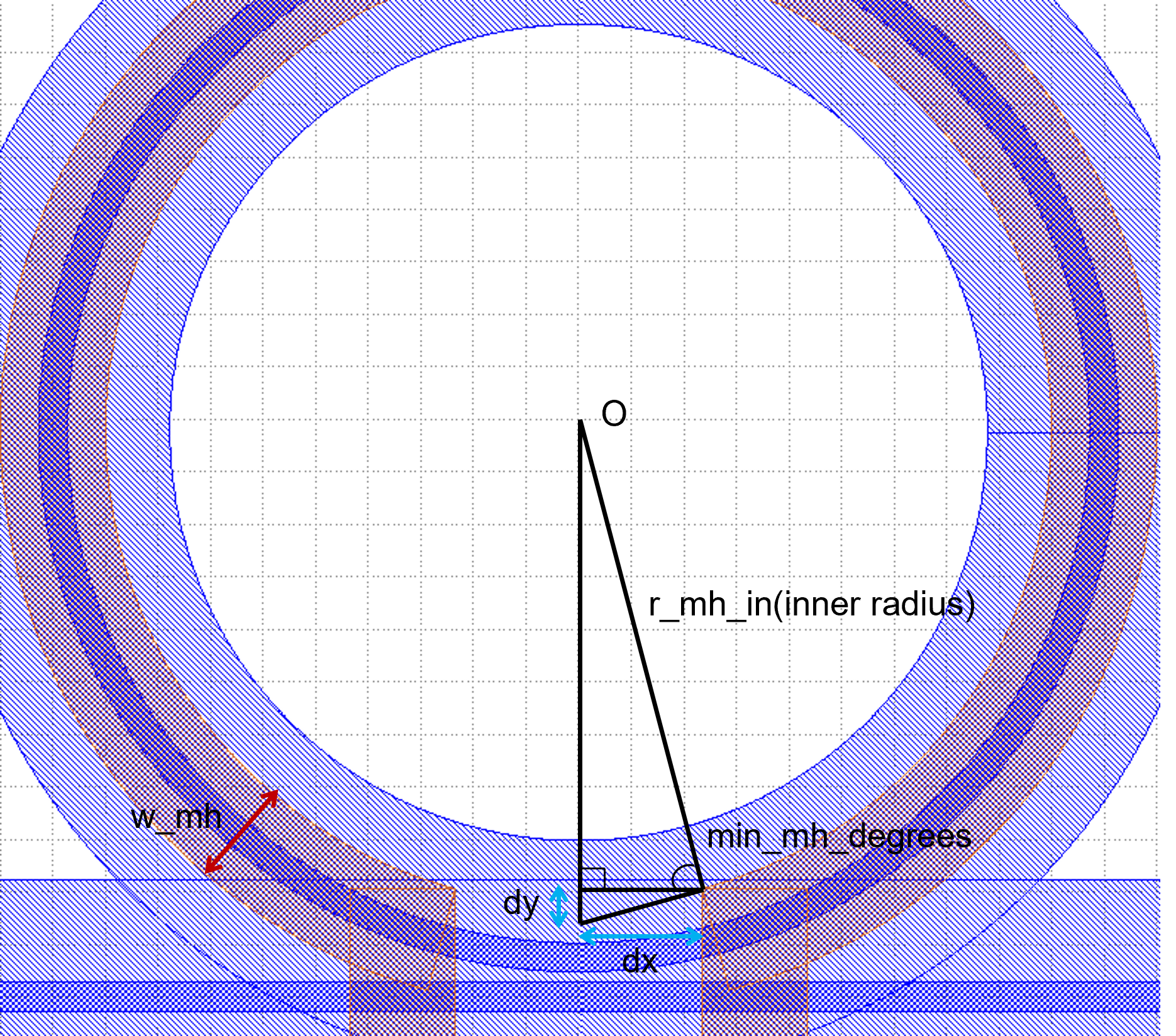
The following diagram illustrates the parameters of r_mh_in, w_mh, min_mh_degrees, dx and dy in the program. It should be noted that the value of min_mh_degrees has a positive or negative nature and needs to be taken into account when designing.
The following code sets the origin of the entire device and adds a ring structure with radius ring_radius to insts, which has no ports structure and is named ring.
x0 = 0
y0 = ring_radius + gap + core_width
ring = waveguide_type(curve=fp.g.EllipticalArc(radius=ring_radius, origin=(x0, y0))).with_ports((None, None)).with_name("ring")
insts += ring
y0 is the radius of the ring + the spacing below + the width of the core, the actual position of the origin of the entire device becomes:
The following code adds four taper structures to the si_etch2_layer layer. length is the total length of the taper, stroke_width can be interpreted as the width of the left end of the taper, and final_stroke_width is the width of the right end.
taper2 = fp.el.Line(length=taper_length, stroke_width=taper_big_end, final_stroke_width=taper_small_end, layer=si_etch2_layer, origin=(x0 + w_si_3 / 2, 0))
elems += taper2
taper3 = fp.el.Line(length=taper_length, stroke_width=taper_big_end, final_stroke_width=taper_small_end, layer=si_etch2_layer, origin=(x0 + w_si_3 / 2, y_offset))
elems += taper3
taper0 = fp.el.Line(length=taper_length, stroke_width=taper_small_end, final_stroke_width=taper_big_end, layer=si_etch2_layer, anchor=fp.Anchor.END, origin=(x0 - w_si_3 / 2, y_offset))
elems += taper0
taper1 = fp.el.Line(length=taper_length, stroke_width=taper_small_end, final_stroke_width=taper_big_end, layer=si_etch2_layer, anchor=fp.Anchor.END, origin=(x0 - w_si_3 / 2, 0))
elems += taper1
ring_mh = fp.el.EllipticalArc(radius=r_mh, stroke_width=w_mh, layer=mh_layer, final_degrees=max_mh_degrees - min_mh_degrees, transform=fp.rotate(degrees=min_mh_degrees).translate(x0, y0))
elems += ring_mh
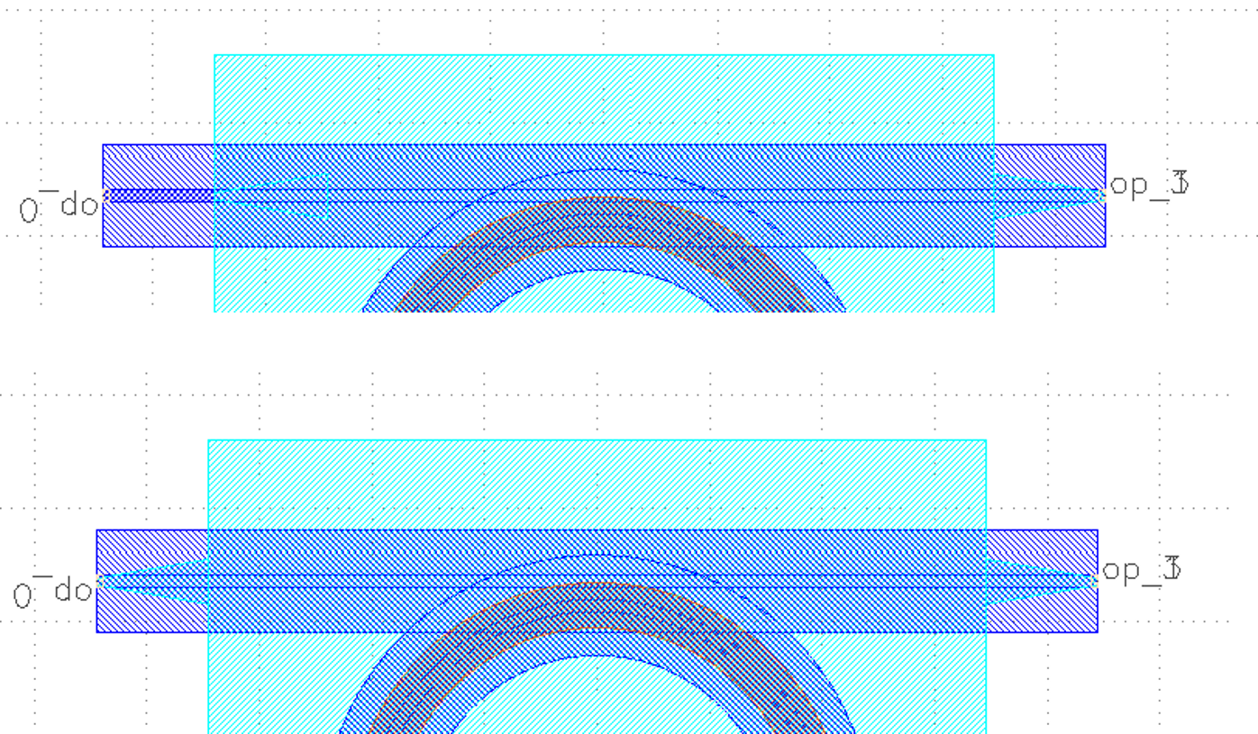
Here we remove the anchor parameter from taper1 and run the result compared with the original result, we can see that the taper has moved. Here the user can interpret this as the origin point is at the center of the right end of the taper when anchor=fp.Anchor.END is not added, and if anchor=fp.Anchor.END is added, the origin point is at the center of the left end of the taper.
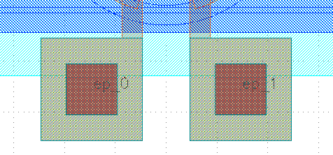
The code below is to add structures on four different layers with the same square structure in two groups in the figure below.
# TODO magic number 10
#VIA1 Layer
v1 = fp.el.Rect(width=via_width, height=via_height, layer=vl_layer, origin=(dx + via_width, -10 + via_height / 2 - core_width / 2))
elems += v1
v2 = fp.el.Rect(width=via_width, height=via_height, layer=vl_layer, origin=(-dx - via_width, -10 + via_height / 2 - core_width / 2))
elems += v2
#M2 Layer
m2 = fp.el.Rect(width=10, height=10, layer=LAYER.M2_DRW, origin=(dx + via_width, -10 + via_height / 2 - core_width / 2))
elems += m2
m2 = fp.el.Rect(width=10, height=10, layer=LAYER.M2_DRW, origin=(-dx - via_width, -10 + via_height / 2 - core_width / 2))
elems += m2
#VIA2 Layer
v1 = fp.el.Rect(width=via_width, height=via_height, layer=LAYER.VIA2_DRW, origin=(dx + via_width, -10 + via_height / 2 - core_width / 2))
elems += v1
v2 = fp.el.Rect(width=via_width, height=via_height, layer=LAYER.VIA2_DRW, origin=(-dx - via_width, -10 + via_height / 2 - core_width / 2))
elems += v2
#MT Layer
mt = fp.el.Rect(width=10, height=10, layer=LAYER.MT_DRW, origin=(dx + via_width, -10 + via_height / 2 - core_width / 2))
elems += mt
mt = fp.el.Rect(width=10, height=10, layer=LAYER.MT_DRW, origin=(-dx - via_width, -10 + via_height / 2 - core_width / 2))
elems += mt
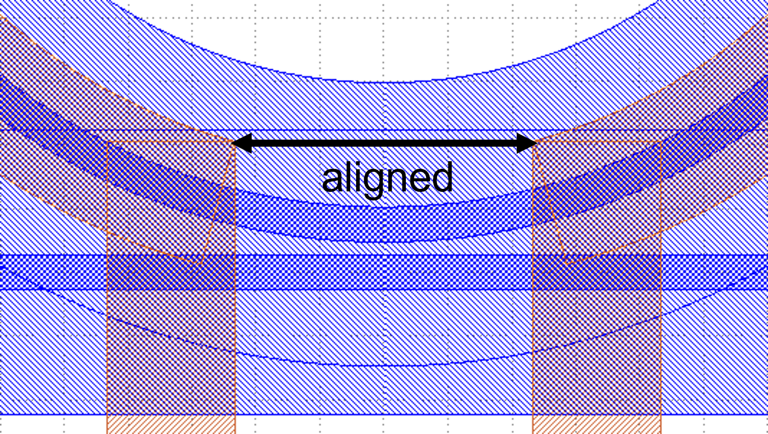
The lower code is responsible for adding the rectangle structure to the mh_layer.
h_mh = y0 + dy + core_width / 2 + via_height / 2
mh1 = fp.el.Rect(width=w_mh, height=h_mh, layer=mh_layer, origin=(dx + w_mh / 2, -core_width / 2 - 2.5 + h_mh / 2))
elems += mh1
mh2 = fp.el.Rect(width=w_mh, height=h_mh, layer=mh_layer, origin=(-dx - w_mh / 2, -core_width / 2 - 2.5 + h_mh / 2))
elems += mh2
Adjust the position of the origin point of the structure so that the lower two positions are aligned.
The code below is to get the location of the six points where the ports needs to be placed, and add the ports by fp.Port and the pins by fp.Pin. In fp.Pin(), set the pins to the same shape (square) as v2, and set the metal wire type to TECH.METAL.MT.W10.
top_start_ray, top_end_ray = monitor.curve.end_rays
bottom_start_ray, bottom_end_ray = bus.curve.end_rays

pin1_x, pin1_y = (-dx - via_width, -10 + via_height / 2 - core_width / 2)
pin2_x, pin2_y = (dx + via_width, -10 + via_height / 2 - core_width / 2)
ports += fp.Port(name=port_names[0], position=top_start_ray.position, orientation=top_start_ray.orientation, waveguide_type=waveguide_type)
ports += fp.Port(name=port_names[1], position=bottom_start_ray.position, orientation=bottom_start_ray.orientation, waveguide_type=waveguide_type)
ports += fp.Port(name=port_names[2], position=bottom_end_ray.position, orientation=bottom_end_ray.orientation, waveguide_type=waveguide_type)
ports += fp.Port(name=port_names[3], position=top_end_ray.position, orientation=top_end_ray.orientation, waveguide_type=waveguide_type)
ports += fp.Pin(name=port_names[4], position=(pin1_x, pin1_y), shape=v1.shape, metal_line_type=TECH.METAL.MT.W10)
ports += fp.Pin(name=port_names[5], position=(pin2_x, pin2_y), shape=v2.shape, metal_line_type=TECH.METAL.MT.W10)
The following diagram illustrates the location of each port and its corresponding port_names.