Define Ports/Pins
When creating Pcells, ports/pins are essential units not only to recognize and define where the input/output of the Pcells are but also to offer the connecting information for the powerful auto-routing function in PhotoCAD.
Ports/Pins from existing PCells
When the PCell already contains some existing PCells with some ports, it is convenient to assign the old port to the port of the new PCell.
If generating a PCell by curve points or line
This often happens when we are creating a PCell with points or lines. First we will create an instance which is a
waveguide_typeand we assign acurveand to thewaveguide_type(waveguide_type(curve=curve).with_port(port_name)). Users can seeStraight,BendorTaperfor more details.Here we call the name of the
waveguide_typewg. Then the ports will be added byports += wg.portssince the position and orientation of the port is already defined when generating the instancewg. The names is added when thewaveguide_typehas the functionwith_port(name=port_name)being defined.The ports generated by
wg.portsfunction should be added to the port container, mostly referred toports.If the existing PCells are instances
This is mostly the common method when generating a new PCell by some existing lower-level PCells. Here the ports are already defined in the old PCells with
nameandposition.To assign the old ports to the ports of the new PCells, we can first call the old port from the old PCell
your_cell_name["op_0"]. Then usewith_namefunction to assign the old ports to the designated name. So the total script will look like:old_cell_name["old_cell_port_name"].with_name("new_cell_port_name")
Now the port information will be transferred to the new PCell.
Manually adding Ports/Pins
Instead of initiating ports/pins from the existing ports of a Pcell(see examples Splitter, Mzm), we can also create ports/pins from fp.Port or fp.Pin, and this allows users to generate ports individually at any places without the restriction of only on the existing Pcells.
This section is a guide to show you how to add ports/pins from fp.Port or fp.Pin function, and we will create a rectangular where one side of the shape is port and another is pin.
Full Script
import math
from typing import Tuple
from gpdk.technology import get_technology, WG
from fnpcell import all as fp


class fpPinPort(fp.PCell):

    height: float = fp.PositiveFloatParam(default=10)
    width: float = fp.PositiveFloatParam(default=50)
    waveguide_type: WG.FWG.C = fp.WaveguideTypeParam(type=WG.FWG.C)
    port_names: fp.IPortOptions = fp.PortOptionsParam(count=2, default=("op_0", "ep_0"))

    def _default_waveguide_type(self):
        return get_technology().WG.FWG.C.WIRE

    def build(self):
        insts, elems, ports = super().build()
        TECH = get_technology()

        rec = fp.el.Rect(height=self.height, width=self.width, center=(0, 0), layer=TECH.LAYER.FWG_CLD)
        elems += rec

        ports += fp.Port(name=self.port_names[0], position=(-self.width/2, 0),
                         waveguide_type=self.waveguide_type.updated(core_layout_width=self.height), orientation=-math.pi)
        ports += fp.Pin(name=self.port_names[1], position=(self.width/2, 0), metal_line_type=TECH.METAL.M1.W10, orientation=0)


        return insts, elems, ports


if __name__ == "__main__":
    from gpdk.util.path import local_output_file

    gds_file = local_output_file(__file__).with_suffix(".gds")
    library = fp.Library()

    TECH = get_technology()
    # =============================================================
    # fmt: off

    library += fpPinPort()

    # fmt: on
    # =============================================================
    fp.export_gds(library, file=gds_file)
    fp.plot(library)
Section Script Description
Importing necessary function packages
To customize the components in gpdk,
fnpcell,typingandmathneed to be imported because modules such as data format, graphics generation, data processing need to be used. Moreover, graphics in the component layout need to be generated on different process layers, so process information(technology,WG) in gpdk needs to be imported:import math from typing import Tuple from gpdk.technology import get_technology, WG from fnpcell import all as fp
Define the properties and methods in the
MzmclassDefine user-definable parameters:
height: float = fp.PositiveFloatParam(default=10)
width: float = fp.PositiveFloatParam(default=50)
port_names: fp.IPortOptions = fp.PortOptionsParam(count=2, default=("op_0", "ep_0"))
heightandwidthare the dimension of the rectangular.port_namesis used to define the number of ports of the component. Secondly, the ports are named, and the default isdefault=("op_0", "op_1"), the user can set it by himself.
Define the build method.
Instances, elements and ports are usually used in device cells, i.e. calls to other cell instances, graphics in this cell and device ports.
The three elements in the device are implemented in the PCell definition by calling the build function module in the parent class PCell:
def build(self):
insts, elems, ports = super().build()
Generate the rectangular geometry as a element by
fp.el.Rectand initiate to the ElementSet(elems).:rec = fp.el.Rect(height=self.height, width=self.width, center=(0, 0), layer=TECH.LAYER.FWG_COR) elems += rec
Generate the ports/pins by
fp.Port/Pin. Note here the name of the ports/pins can be named by the users (type should bestr).positioncan also be adjust byat, e.g.at=component["op_0], to assign a new port to the existing portports += fp.Port(name=self.port_names[0], position=(-self.width/2, 0), waveguide_type=TECH.WG.FWG.C.WIRE.updated(core_layout_width=self.height), orientation=-math.pi) ports += fp.Pin(name=self.port_names[1], position=(self.width/2, 0), metal_line_type=TECH.METAL.M1.W10, orientation=0)
Return the instances, elements, and ports in the component cell.
return insts, elems, ports
View the layout
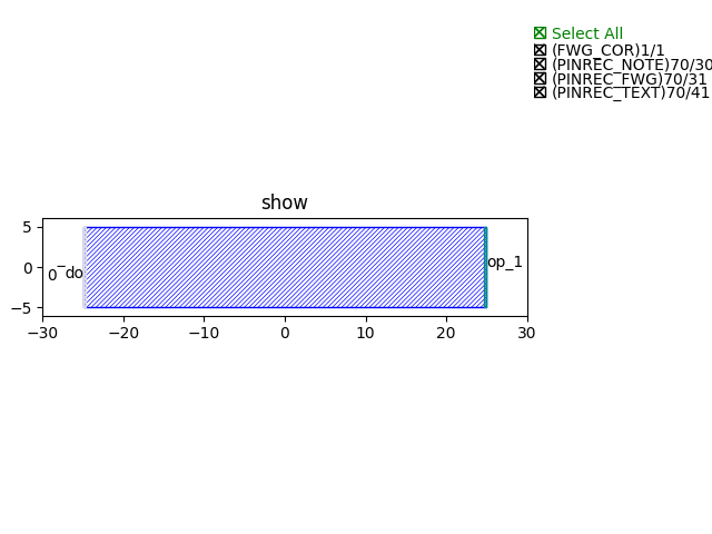
We can see from the above figure that we have created a rectangular with height=10, width=50. The left port named op_0 is an optical port with a width = 10, and the right port named ep_0 is then an electrical port with also a width = 10. The two ports which we defined individually are able to recognize by the auto-routing function.