Design rule check(DRC)
What is DRC?
Design Rule Check (DRC) is a crucial step in the photonics/electronic design automation (EDA) process for photonics integrated circuits (PICs). It is a verification process that ensures the compliance of a photonics layout or design with a set of predefined rules and constraints. The primary goal of DRC is to identify and rectify potential issues or violations in the layout that could lead to manufacturing defects, reliability issues, or functional failures in the final product.
DRC is an integral part of the PICs design flow, typically performed after the completion of the physical layout but before the fabrication process begins. It helps ensure that the design adheres to the specifications provided by the foundry or fabrication facility.
Most common type of design rules are:
Other rules provided by specific foundries
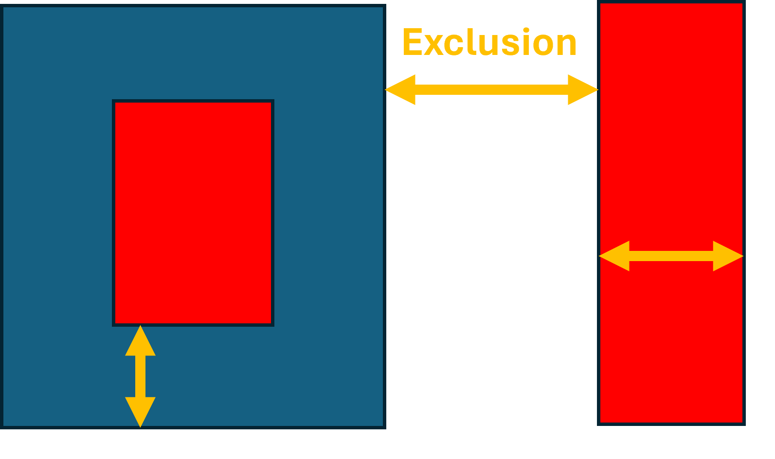
Exclusion
Specifies the minimum allowable distance between adjacent features (such as waveguides, metal layers) to prevent optical crosstalk or electrical interference
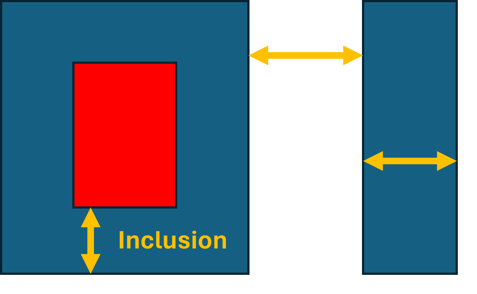
Inclusion
Specifies the minimum distance between the edge of a feature and the nearest edge of an adjacent feature, ensuring proper isolation.
Minimum_width
Defines the minimum allowable width for waveguides or other features to ensure proper functionality and manufacturability.

DRC check in KLayout
View designs in KLayout
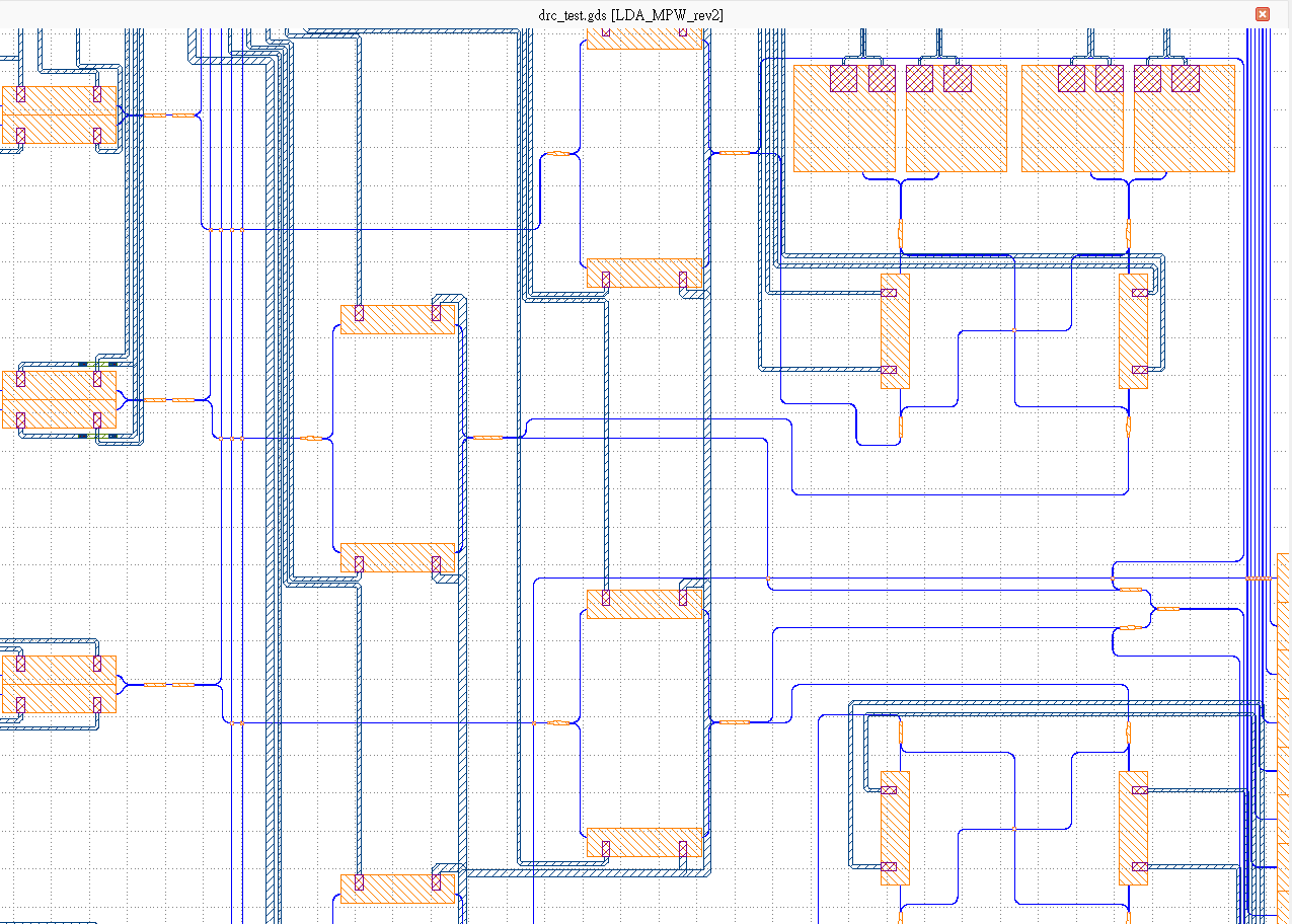
After designing your chip in PhotoCAD, a GDS file will be generated and you can view your designs in a license-free software KLayout. For example, here we show a complicated circuit with complex waveguide and metal routing.
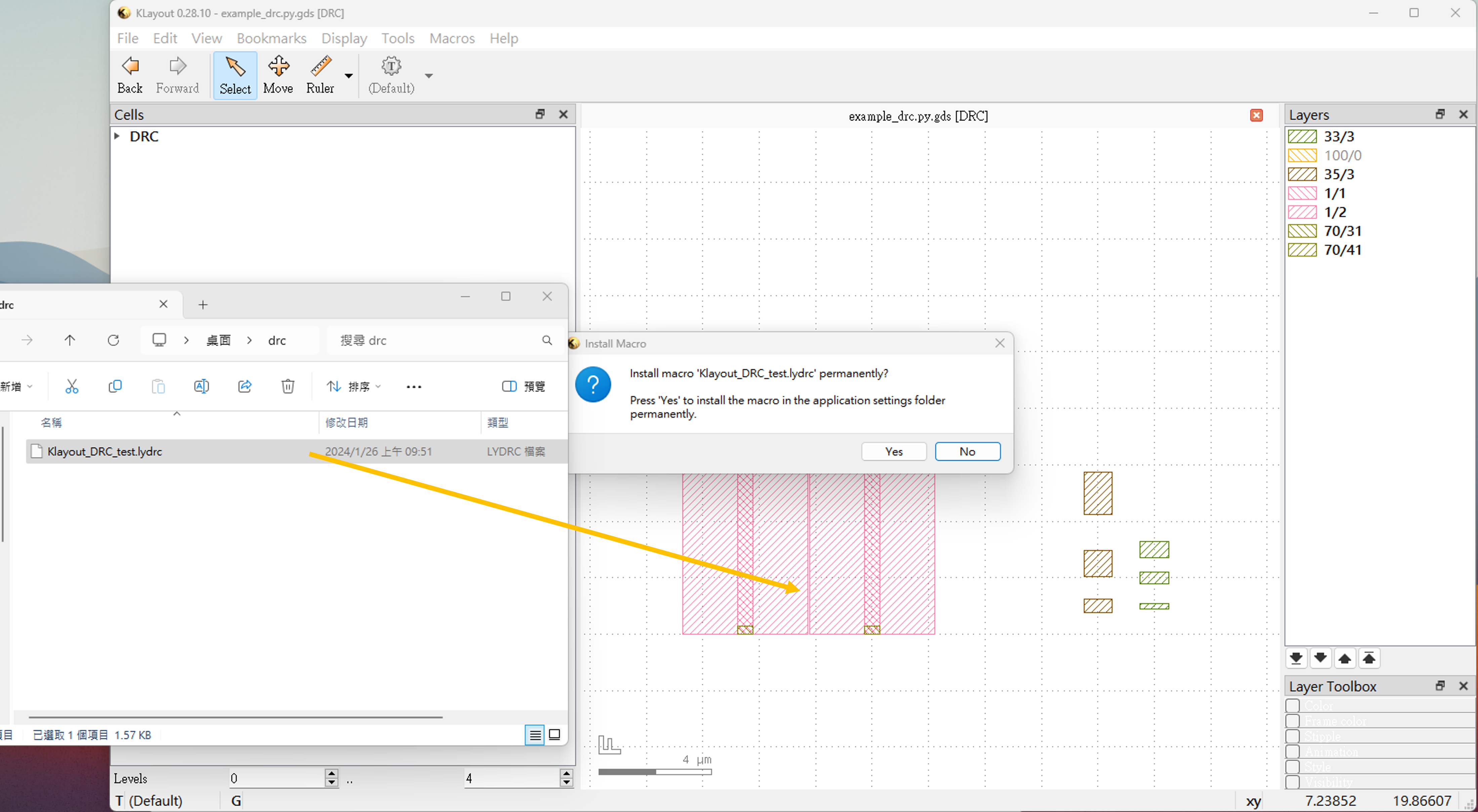
Import DRC file to KLayout
Next, select the “DRC” from “Tools” and import the DRC file (.lydrc) of the specific foundry. It can be easily done by dragging the file into KLayout layout view window and install the macro. DRC file contains a set of instructions and parameters that define the design rules and constraints to be verified during the DRC process. This file serves as input to KLayout, guiding the verification process and enabling the tool to check the physical layout against the specified criteria.
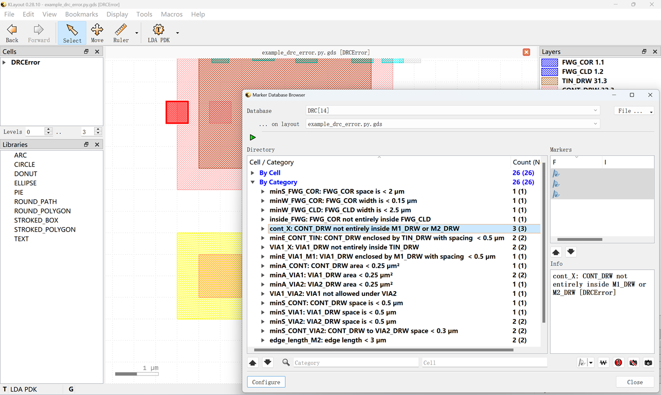
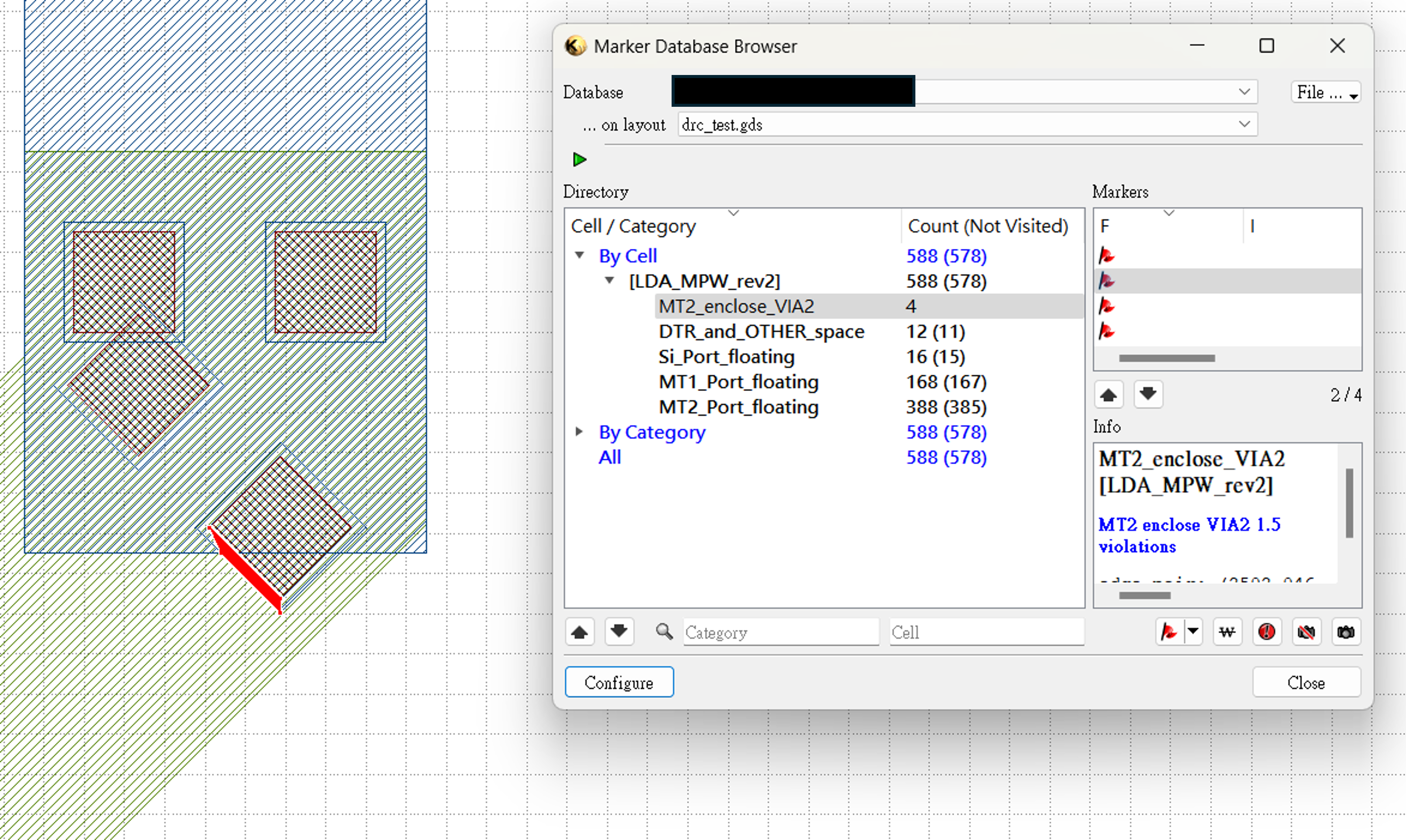
View design rule errors
After the DRC process is done, a DRC result file will be exported and you can those errors in the “Marker Browser” from “Tools”.
All errors from the same rule will be collected together and will be marked red in the layout.
Make adjustments or waive the error
Then, it is time to make necessary adjustments to the layout to correct the identified violations. This may involve modifying the placement, dimensions, or other characteristics of the components to ensure compliance with the design rules.
Design rule check often need to be done several times until the layout is error-free and meets all design rule requirements. Sometimes it is possible to waive the errors and it must be done after discussion with the foundry.
Examples files to test your knowledge
Here we provide a simple DRC file and an example GDS layout for ou to test your knowledge and get a glimpse of how design rule checking is done in KLayout.
In the Klayout_DRC_test.lydrc file, we’ve set up rules for the minimum width and spacing of layers like FWG, M1, and M2. These rules use the input function to assign layer numbers based on the recognized layer names, making it easy to check designs in KLayout.
minW_FWG = 0.15
minS_FWG = 0.15

minW_M1 = 0.3
minS_M1 = 0.6

minW_M2 = 0.9
minS_M2 = 0.9

FWG_COR = input(1,1)
FWG_CLD = input(1,2)
FWG_TRE = input(1,4)

M1_DRW = input(33,3)
M2_DRW = input(35,3)

FWG = (FWG_CLD - FWG_COR) or FWG_TRE
M1 = M1_DRW
M2 = M2_DRW
FWG.width(minW_FWG).output("FWG width violation")
M1.width(minW_M1).output("M1 width violation")
M2.width(minW_M2).output("M2 width violation")

FWG.space(minS_FWG).output("FWG space violation")
M1.space(minS_M1).output("M1 space violation")
M2.space(minS_M2).output("M2 space violation")
In the example GDS layout file, we’ve created different shapes on layers FWG, M1, and M2 to demonstrate how the rules work. Some shapes follow the design rules, while others don’t. In real design work, it’s crucial for designers to consider and follow the specific design rules provided by foundries. This helps ensure that the circuit designs are reliable and function as intended.
After running the above example file, we can learn more scripts to enrich the design rules, below we show more examples of DRC scripts and their corresponding layout situations:
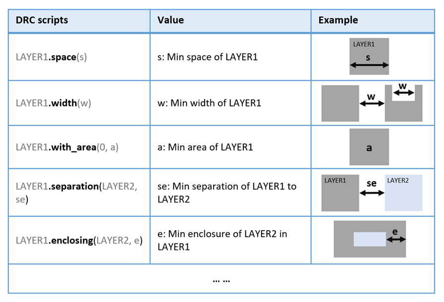
More design rules can be found on the Klayout website: https://klayout.org/downloads/master/doc-qt5/about/drc_ref.html
We have also prepared additional DRC sample layout and scripts which use more design rules and also enrich the return message writing after checking, you can download the layout file and DRC script file below, run them and check for errors.