Programmable Photonic Integrated Circuit
Programmable photonic circuits are an important discipline in the development of photonics, and this section focuses on how to build reconfigurable programmable photonic circuits in detail.
This section aims to build reconfigurable rectangular optical networks using rectangular networks as an example. The reconfigurable parameters include:
Basic Module
Network Size
Design Parameters
Part I. Building a Rectangular Network
Importing library files:
from typing import Mapping, cast

from fnpcell import all as fp
from gpdk.technology import get_technology
from ring_modulator import RingModulator
from h_fanout import HFanout
from gpdk.technology.waveguide_factory import EulerBendFactory
Define class PICircuit:
class PICircuit(fp.PCell):
    def build(self):
        global spacing
        insts, elems, ports = super().build()
        TECH = get_technology()

        row_number = 100
        column_number = 100
        basic_comp = RingModulator()
        basic_comp_y = RingModulator(transform=fp.rotate(degrees=90))

        xy_spacing = []
        xx_spacing = []
        yy_spacing = []
        yx_spacing = []

        for i in range(row_number + 1):
            xy_spacing.append(spacing * i)

        for i in range(column_number):
            xx_spacing.append(spacing * (i + 0.5))

        for i in range(row_number):
            yy_spacing.append(spacing * (i + 0.5))

        for i in range(column_number + 1):
            yx_spacing.append(spacing * i)

        x_straight_top_right = []
        x_straight_btm_right = []
        x_straight_top_left = []
        x_straight_btm_left = []
        straight_index_min_x = 0
        straight_index_max_x = 0
        straight_index_min_xt = 0
        straight_index_max_xt = 0

        for i in range(row_number + 1):
            for j in range(column_number):
                x = xx_spacing[j]
                y = xy_spacing[i]
                x_dcoupler = basic_comp["op_0"].repositioned(at=(x, y)).owner
                insts += x_dcoupler, f"{0},{i},{j}"
                if (i == 0) and (j == 0):
                    get_position_y = basic_comp["op_1"].position[y]
                    x_straight_btm_left.append(pdk.Straight(name = "xbl_straight"+str(straight_index_min_x) ,length=20, waveguide_type=TECH.WG.FWG.C.WIRE)["op_0"].repositioned(at=(x-30-0.5*spacing, get_position_y)).owner)
                    insts += x_straight_btm_left[straight_index_min_x], f"{4},{0},{straight_index_min_x}"
                    straight_index_min_x = straight_index_min_x+1
                if (i == 0) and (j == (column_number-1)):
                    get_position_y = basic_comp["op_1"].position[y]
                    x_straight_btm_right.append(pdk.Straight(name = "xbr_straight"+str(straight_index_max_x) ,length=20, waveguide_type=TECH.WG.FWG.C.WIRE)["op_0"].repositioned(at=(x+60+0.5*spacing, get_position_y)).owner)
                    insts += x_straight_btm_right[straight_index_max_x], f"{4},{1},{straight_index_max_x}"
                    straight_index_max_x = straight_index_max_x+1
                if (i == row_number) and (j == 0):
                    x_straight_top_left.append(pdk.Straight(name = "xtl_straight"+str(straight_index_min_xt) ,length=20, waveguide_type=TECH.WG.FWG.C.WIRE)["op_0"].repositioned(at=(x-30-0.5*spacing, y)).owner)
                    insts += x_straight_top_left[straight_index_min_xt], f"{5},{0},{straight_index_min_xt}"
                    straight_index_min_xt = straight_index_min_xt+1
                if (i == row_number) and (j == (column_number-1)):
                    x_straight_top_right.append(pdk.Straight(name = "xtr_straight"+str(straight_index_max_xt) ,length=20, waveguide_type=TECH.WG.FWG.C.WIRE)["op_0"].repositioned(at=(x+60+0.5*spacing,y)).owner)
                    insts += x_straight_top_right[straight_index_max_xt], f"{5},{1},{straight_index_max_xt}"
                    straight_index_max_xt = straight_index_max_xt+1


        y_straight_top_right = []
        y_straight_btm_right = []
        y_straight_top_left = []
        y_straight_btm_left = []
        straight_index_min = 0
        straight_index_max = 0

        for i in range(row_number):
            for j in range(column_number + 1):
                x = yx_spacing[j]
                y = yy_spacing[i]
                y_dcoupler = basic_comp_y["op_0"].repositioned(at=(x, y)).owner
                insts += y_dcoupler, f"{1},{i},{j}"
                if (j == 0) :
                    y_straight_top_right.append(pdk.Straight(name = "tr_straight"+str(straight_index_min) ,length=20, waveguide_type=TECH.WG.FWG.C.WIRE)["op_0"].repositioned(at=(x-30, y+60)).owner)
                    y_straight_btm_right.append(pdk.Straight(name = "br_straight"+str(straight_index_min) ,length=20, waveguide_type=TECH.WG.FWG.C.WIRE)["op_0"].repositioned(at=(x-30, y-10)).owner)
                    insts += y_straight_top_right[straight_index_min], f"{2},{0},{straight_index_min}"
                    insts += y_straight_btm_right[straight_index_min], f"{2},{1},{straight_index_min}"
                    straight_index_min = straight_index_min+1
                if (j == (column_number)) :
                    y_straight_top_left.append(pdk.Straight(name = "tl_straight"+str(straight_index_max) ,length=10, waveguide_type=TECH.WG.FWG.C.WIRE)["op_0"].repositioned(at=(x+60, y+60)).owner)
                    y_straight_btm_left.append(pdk.Straight(name = "bl_straight"+str(straight_index_max) ,length=10, waveguide_type=TECH.WG.FWG.C.WIRE)["op_0"].repositioned(at=(x+60, y-10)).owner)
                    insts += y_straight_top_left[straight_index_max], f"{3},{0},{straight_index_max}"
                    insts += y_straight_btm_left[straight_index_max], f"{3},{1},{straight_index_max}"
                    straight_index_max = straight_index_max+1

        progcuit = cast(Mapping[str, fp.ICellRef], insts)
        # p = progcuit["0,1,3"]["op_2"].position[0]

        for i in range(row_number + 1):
            for j in range(column_number):
                if i == 0 and (j < column_number - 1):
                    link1 = fp.LinkBetween(start=progcuit[f"{0},{i},{j}"]["op_2"],
                                           end=progcuit[f"{0},{i},{j + 1}"]["op_1"],
                                           bend_factory=EulerBendFactory(radius_min=5, l_max=5, waveguide_type=TECH.WG.FWG.C.WIRE))
                    insts += link1
                if i == row_number and (j < column_number - 1):
                    link2 = fp.LinkBetween(start=progcuit[f"{0},{i},{j}"]["op_3"],
                                           end=progcuit[f"{0},{i},{j + 1}"]["op_0"],
                                           bend_factory=EulerBendFactory(radius_min=5, l_max=15, waveguide_type=TECH.WG.FWG.C.WIRE))
                    insts += link2
                if (i < row_number) and (j < column_number):
                    link3 = fp.LinkBetween(start=progcuit[f"{0},{i},{j}"]["op_0"],
                                           end=progcuit[f"{1},{i},{j}"]["op_1"],
                                           bend_factory=EulerBendFactory(radius_min=5, l_max=15, waveguide_type=TECH.WG.FWG.C.WIRE))
                    insts += link3
                    link4 = fp.LinkBetween(start=progcuit[f"{0},{i},{j}"]["op_3"],
                                           end=progcuit[f"{1},{i},{j + 1}"]["op_0"],
                                           bend_factory=EulerBendFactory(radius_min=15, l_max=15, waveguide_type=TECH.WG.FWG.C.WIRE))
                    insts += link4
                    link5 = fp.LinkBetween(start=progcuit[f"{0},{i + 1},{j}"]["op_1"],
                                           end=progcuit[f"{1},{i},{j}"]["op_2"],
                                           bend_factory=EulerBendFactory(radius_min=15, l_max=15, waveguide_type=TECH.WG.FWG.C.WIRE))
                    insts += link5
                    link6 = fp.LinkBetween(start=progcuit[f"{0},{i + 1},{j}"]["op_2"],
                                           end=progcuit[f"{1},{i},{j + 1}"]["op_3"],
                                           bend_factory=EulerBendFactory(radius_min=15, l_max=15, waveguide_type=TECH.WG.FWG.C.WIRE))
                    insts += link6
        n = 0
        link7 = fp.LinkBetween(start=progcuit[f"{0},{0},{column_number-1}"]["op_2"],
                               end=progcuit[f"{4},{1},{0}"]["op_0"],
                               bend_factory=TECH.WG.FWG.C.WIRE.BEND_CIRCULAR)
        insts += link7
        ports += progcuit[f"{4},{1},{0}"]["op_1"].with_name("op_"+str(n))

        for i in range(row_number):
            link8 = fp.LinkBetween(start=progcuit[f"1,{i},{column_number}"]["op_1"],
                                   end=progcuit[f"{3},{1},{i}"]["op_0"],
                                   bend_factory=EulerBendFactory(radius_min=15, l_max=15, waveguide_type=TECH.WG.FWG.C.WIRE))
            insts += link8
            n = n + 1
            ports += progcuit[f"{3},{1},{i}"]["op_1"].with_name("op_"+str(n))
            link9 = fp.LinkBetween(start=progcuit[f"1,{i},{column_number}"]["op_2"],
                                   end=progcuit[f"{3},{0},{i}"]["op_0"],
                                   bend_factory=EulerBendFactory(radius_min=15, l_max=15, waveguide_type=TECH.WG.FWG.C.WIRE))
            insts += link9
            n = n + 1
            ports += progcuit[f"{3},{0},{i}"]["op_1"].with_name("op_"+str(n))

        n = n + 1
        link10 = fp.LinkBetween(start=progcuit[f"{0},{row_number},{column_number-1}"]["op_3"],
                               end=progcuit[f"{5},{1},{0}"]["op_0"],
                               bend_factory=EulerBendFactory(radius_min=15, l_max=15, waveguide_type=TECH.WG.FWG.C.WIRE))
        insts += link10
        ports += progcuit[f"{5},{1},{0}"]["op_1"].with_name("op_"+str(n))

        n = n+1
        link10 = fp.LinkBetween(start=progcuit[f"{0},{row_number},0"]["op_0"],
                               end=progcuit[f"{5},{0},{0}"]["op_1"],
                               bend_factory=EulerBendFactory(radius_min=15, l_max=15, waveguide_type=TECH.WG.FWG.C.WIRE))
        insts += link10
        ports += progcuit[f"{5},{0},{0}"]["op_0"].with_name("op_"+str(n))

        for i in range(row_number-1,-1,-1):
            n = n + 1
            link11 = fp.LinkBetween(start=progcuit[f"1,{i},0"]["op_3"],
                                    end=progcuit[f"{2},{0},{i}"]["op_1"],
                                    bend_factory=EulerBendFactory(radius_min=15, l_max=15,
                                                                  waveguide_type=TECH.WG.FWG.C.WIRE))
            insts += link11
            ports += progcuit[f"{2},{0},{i}"]["op_0"].with_name("op_"+str(n))
            n = n + 1
            link12 = fp.LinkBetween(start=progcuit[f"1,{i},0"]["op_0"],
                                    end=progcuit[f"{2},{1},{i}"]["op_1"],
                                    bend_factory=EulerBendFactory(radius_min=15, l_max=15,
                                                                  waveguide_type=TECH.WG.FWG.C.WIRE))
            insts += link12
            ports += progcuit[f"{2},{1},{i}"]["op_0"].with_name("op_"+str(n))

        n = n+1
        link13 = fp.LinkBetween(start=progcuit["0,0,0"]["op_1"],
                               end=progcuit[f"{4},{0},{0}"]["op_1"],
                               bend_factory=TECH.WG.FWG.C.WIRE.BEND_CIRCULAR)
        insts += link13
        ports += progcuit[f"{4},{0},{0}"]["op_0"].with_name("op_"+str(n))

        # fmt: on
        return insts, elems, ports
Call the main function and use the Hfanout function to implement the grating coupler design:
if __name__ == "__main__":
    from pathlib import Path

    gds_file = Path(__file__).parent / "local" / Path(__file__).with_suffix(".gds").name
    library = fp.Library()

    TECH = get_technology()
    # =============================================================
    # fmt: off

    def bend_factories(waveguide_type: fp.IWaveguideType):
        if waveguide_type == TECH.WG.FWG.C.WIRE:
            return EulerBendFactory(radius_min=15, l_max=15, waveguide_type=waveguide_type)
        return waveguide_type.bend_factory

    library += [
            HFanout(name="mmi",
                    device=PICircuit(),
                    left_spacing=100,
                    right_spacing=100,
                    left_distance=100,
                    right_distance=100,
                    bend_factories=bend_factories,
                    left_waveguide_type=TECH.WG.SWG.C.WIRE,
                    right_waveguide_type=TECH.WG.SWG.C.WIRE)
        ]

    # fmt: on
    # =============================================================
    fp.export_gds(library, file=gds_file)
    fp.plot(library)
Part II. Parameter Description
row_number: Number of horizontal grids of optical networkcolumn_number: Number of vertical grids of optical networkbasic_comp: The base module device, chosen here is the microring modulatorspacing: Component spacing setting
Part III. Test Description
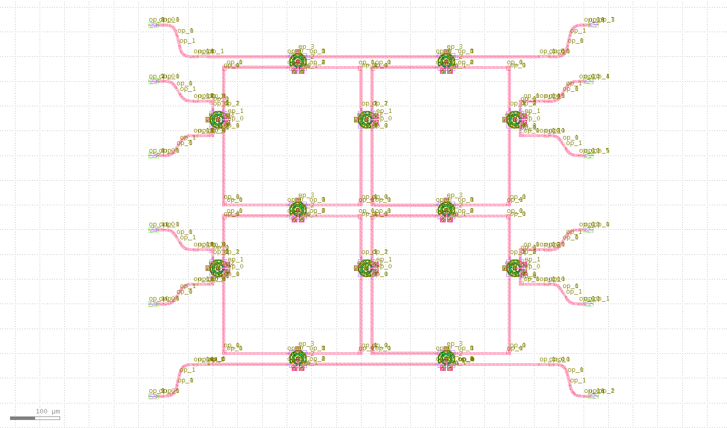
First, a 2*2 square network:
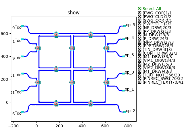
The automatic generation of the layout is shown below:
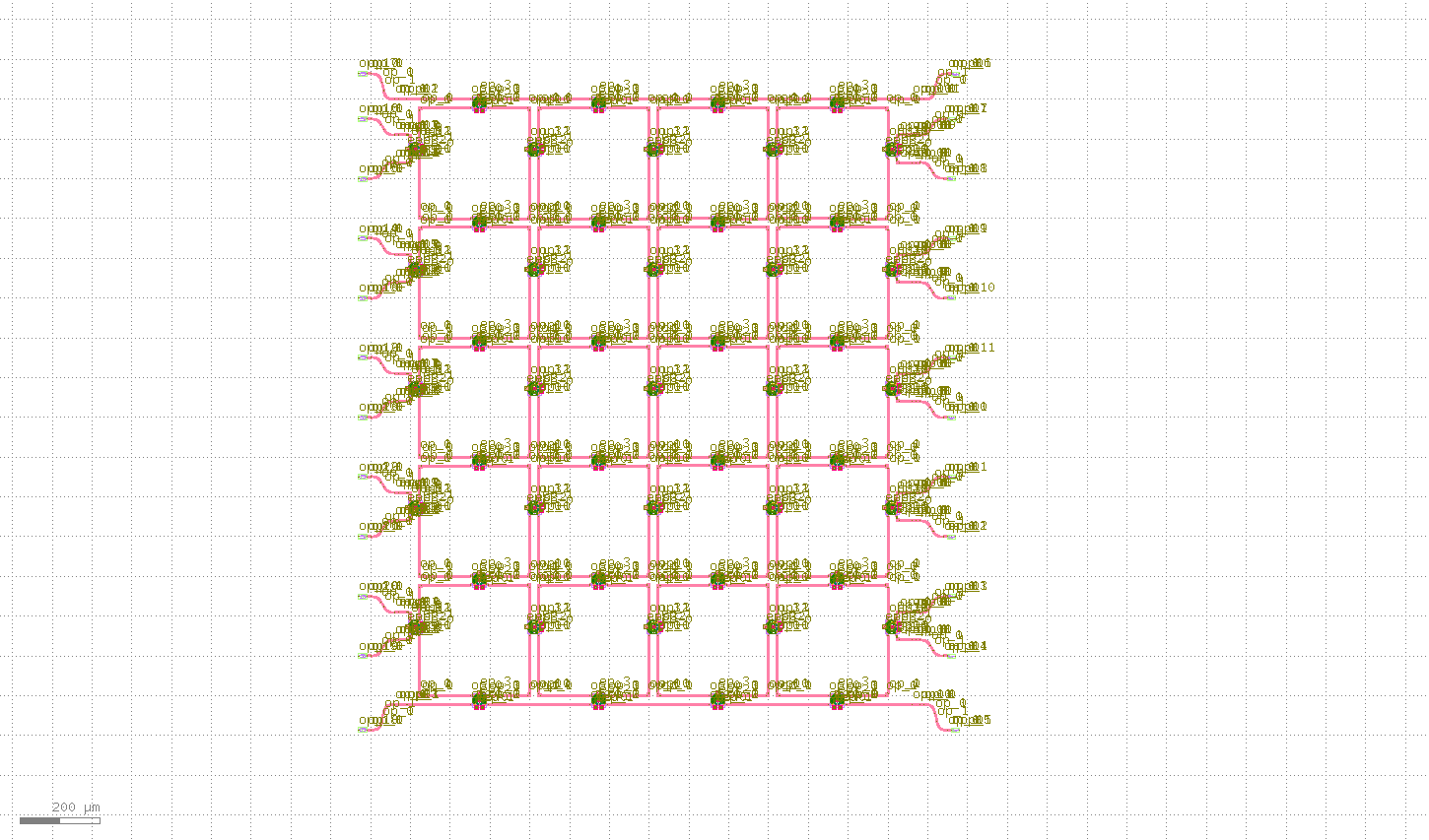
Continue testing 5*4 rectangular network:
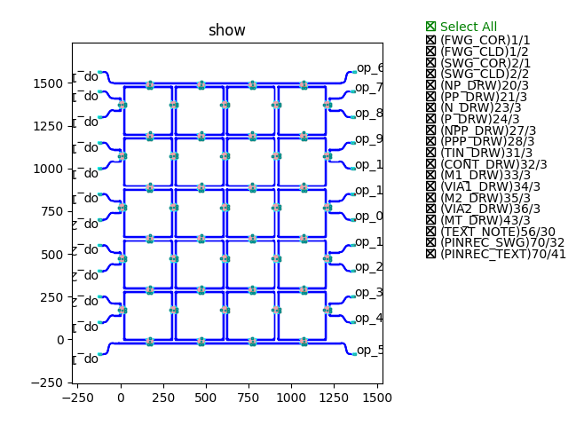
The automatic generation of the layout is shown below:
Finally, to demonstrate the great potential of PhotoCAD in the field of programmable photonic integrated link design, we designed a 20*30 optical network as well as a 100*100 optical network.
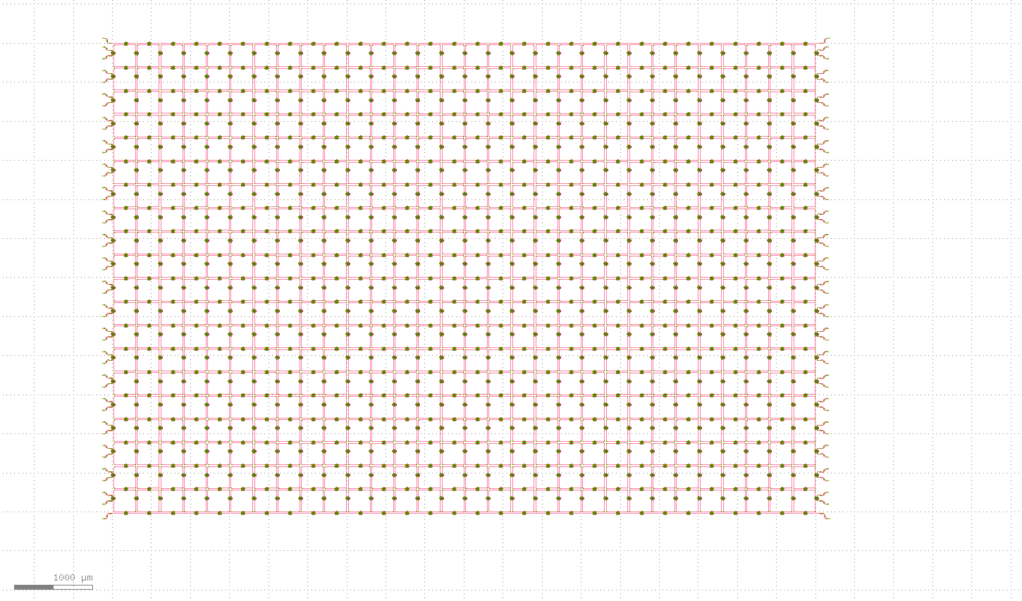

Part IV. Summary
PhotoCAD designs massively programmable photonic circuit plates with excellent performance, and according to the official reconfigurable code provided, we can easily implement various complex networks.